The rapid development of the electronic information industry has enabled electronic products to develop in the direction of miniaturization, functionalization, high performance, and high reliability. From the general surface mount technology (SMT) in the mid-1970s to the high-density interconnect surface mount technology (HDI) in the 1990s, as well as the application of various new packaging technologies such as semiconductor packaging and IC packaging technology that have emerged in recent years, Electronic installation technology continues to develop in the direction of high density. At the same time, the development of high-density interconnect technology promotes the development of PCBs in the direction of high density. With the development of mounting technology and PCB technology, the technology of copper clad laminate as a PCB substrate material is also constantly improving.
Experts predict that the world's electronic information industry will grow at an average annual growth rate of 7.4% in the next 10 years. By 2010, the world's electronic information industry market will reach 3.4 trillion U.S. dollars, of which the electronic complete machine will be 1.2 trillion U.S. dollars, and communication equipment and computers will account for More than 70% of them amounted to 0.86 trillion U.S. dollars. It can be seen that the huge market for copper clad laminates as electronic basic materials will not only continue to exist, but also continue to develop at a growth rate of 15%. The relevant information released by the Copper Clad Laminate Industry Association shows that in the next five years, in order to adapt to the development trends of high-density BGA technology and semiconductor packaging technology, the proportion of high-performance thin FR-4 and high-performance resin substrates will increase.
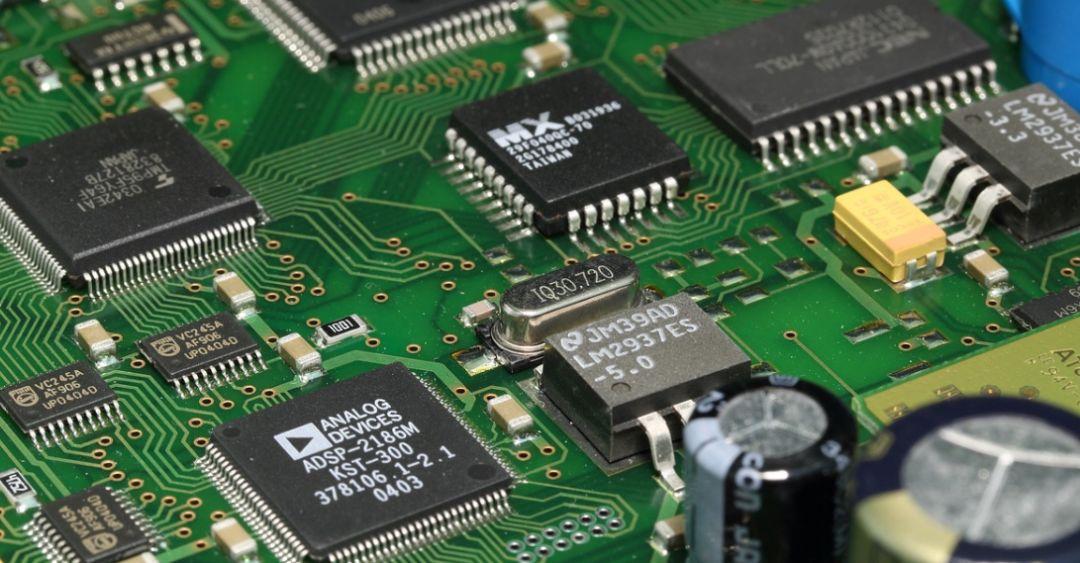
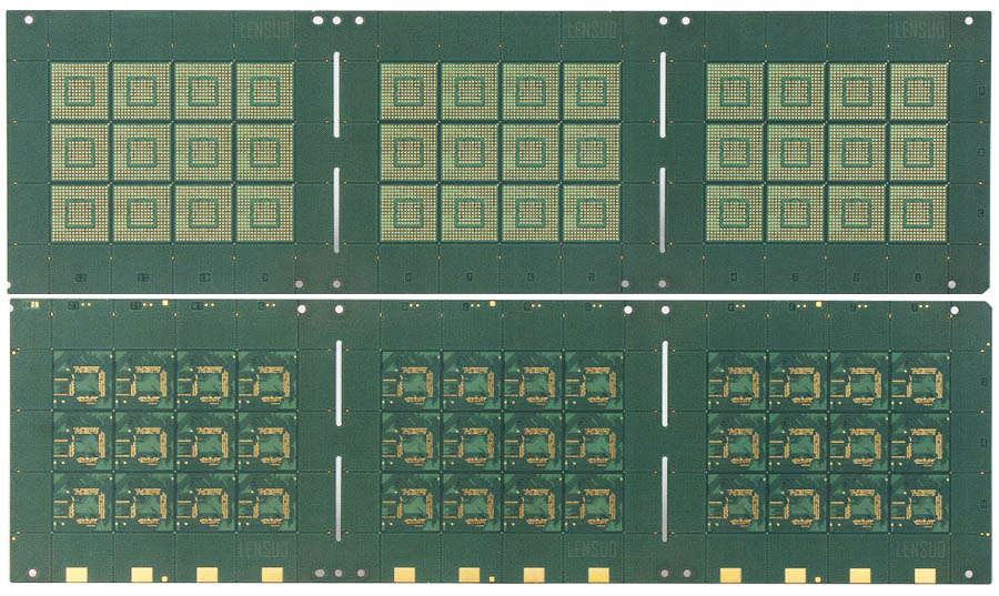
Copper Clad Laminate (CCL), as the substrate material in PCB manufacturing, mainly plays the role of interconnection, insulation and support to the PCB, and has a great impact on the transmission speed, energy loss, and characteristic impedance of the signal in the circuit. Therefore, the PCB The performance, quality, processability in manufacturing, manufacturing level, manufacturing cost, and long-term reliability and stability of CCL depend to a large extent on the material of the copper clad laminate.
CCL technology and production have gone through more than half a century of development. Now the world's annual output of CCL has exceeded 300 million square meters, and CCL has become an important part of basic materials in electronic information products. The copper clad laminate manufacturing industry is a sunrise industry. It has broad prospects along with the development of electronic information and communication industries. Its manufacturing technology is a high-tech that intersects, penetrates, and promotes multiple disciplines. The development history of electronic information technology shows that copper clad laminate technology is one of the key technologies that promote the rapid development of the electronics industry.
The key tasks of my country's copper clad laminate (CCL) industry in the future development strategy. In terms of products, efforts should be made on five types of new PCB substrate materials, that is, through the development of five types of new substrate materials and technological breakthroughs., So that the cutting-edge technology of my country's CCL has been improved. The development of the five types of new high-performance CCL products listed below is a key topic that engineers and technicians in my country's copper clad laminate industry should pay attention to in future research and development.

1. Lead-free compatible copper clad laminate
At the European Union's meeting on October 11, 2002, two "European Directives" on environmental protection content were passed. They will formally implement the resolution on July 1, 2006. The two "European Directives" refer to the "Electrical and Electronic Product Waste Directive" (referred to as WEEE) and the "Restriction Order on the Use of Certain Hazardous Substances" (referred to as RoHs). In these two statutory directives, the requirements are clearly mentioned. The use of lead-containing materials is prohibited. Therefore, the best way to respond to these two directives is to develop lead-free copper clad laminates as soon as possible.
2. High performance copper clad laminate
The high-performance copper clad laminates referred to here include low dielectric constant (Dk) copper clad laminates, copper clad laminates for high frequency and high speed PCBs, high heat resistance copper clad laminates, and various substrate materials for multi-layer laminates (resin coated copper Foil, organic resin film that constitutes the insulating layer of laminated multilayer board, glass fiber reinforced or other organic fiber reinforced prepreg, etc.). In the next few years (to 2010), in the development of this type of high-performance copper clad laminates, according to the forecasted future development of electronic installation technology, the corresponding performance index values should be reached.
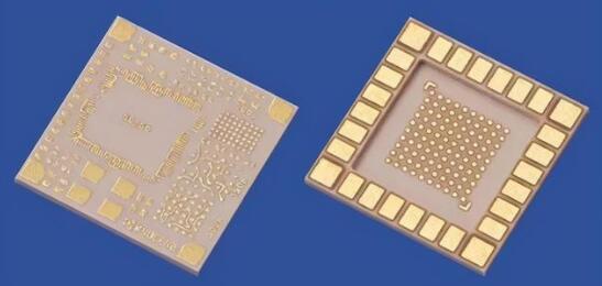
3. Substrate material for IC package carrier board
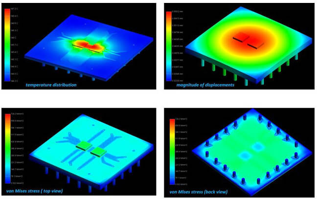
The development of substrate materials for IC packaging substrates (also known as IC packaging substrates) is currently a very important topic. It is also an urgent need to develop my country's IC packaging and microelectronics technology. With the development of IC packaging in the direction of high frequency and low power consumption, IC packaging substrates will be improved in important properties such as low dielectric constant, low dielectric loss factor, and high thermal conductivity. An important subject of future research and development is the effective thermal coordination and integration of substrate thermal connection technology-heat dissipation.
In order to ensure the freedom of IC packaging design and the development of new IC packaging technology, it is indispensable to carry out model tests and simulation tests. These two tasks are very meaningful for mastering the characteristic requirements of substrate materials for IC packaging, that is, understanding and mastering its electrical performance, heat and heat dissipation performance, reliability and other requirements. In addition, it should further communicate with the IC packaging design industry to reach a consensus. The performance of the developed substrate material will be provided to the designer of the complete electronic product in time, so that the designer can establish an accurate and advanced data foundation.
The IC package carrier also needs to solve the problem of inconsistency in the coefficient of thermal expansion with the semiconductor chip. Even with the build-up multilayer board suitable for the production of micro-circuits, the thermal expansion coefficient of the insulating substrate is generally too large (generally, the thermal expansion coefficient is 60ppm/°C). The thermal expansion coefficient of the substrate reaches about 6 ppm, which is close to that of the semiconductor chip, which is indeed a "difficult challenge" for the manufacturing technology of the substrate.
In order to adapt to the development of high speed, the dielectric constant of the substrate should reach 2.0, and the dielectric loss factor can be close to 0.001. For this reason, a new generation of printed circuit boards that exceed the boundaries of traditional substrate materials and traditional manufacturing processes are predicted to appear in the world around 2005. The breakthrough in technology, first of all, is the breakthrough in the use of new substrate materials.
To predict the future development of IC packaging design and manufacturing technology, there are more stringent requirements for the substrate materials used in it. This is mainly manifested in the following aspects: 1. High Tg corresponding to lead-free flux. 2. Achieve low dielectric loss factor matching the characteristic impedance. 3. Low dielectric constant corresponding to high speed (ε should be close to 2). 4. Low warpage (improve the flatness of the substrate surface). 5. Low moisture absorption rate. 6. Low thermal expansion coefficient, so that the thermal expansion coefficient is close to 6ppm. 7. Low cost of IC package carrier. 8. Low-cost substrate material with built-in components. 9. In order to improve the thermal shock resistance, the basic mechanical strength is improved. It is suitable for the substrate material that does not reduce the performance under the temperature change cycle from high to low. 10. A low-cost green substrate material suitable for high reflow soldering temperature.
Four, copper clad laminates with special functions
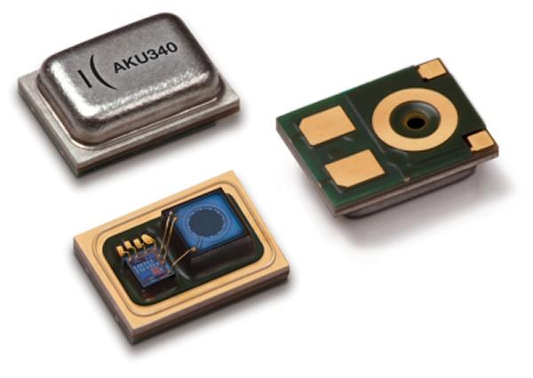
The copper clad laminates with special functions referred to here mainly refer to: metal-based (core) copper clad laminates, ceramic-based copper clad laminates, high-dielectric constant laminates, copper clad laminates (or substrate materials) for embedded passive component-type multilayer boards, Copper-clad laminates for optical-electric circuit substrates, etc. The development and production of this type of copper clad laminate is not only required for the development of new technologies for electronic information products, but also for the development of my country's aerospace and military industries.
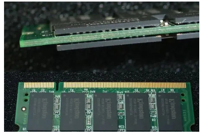
Five, high-performance flexible copper clad laminate
Since the large-scale industrial production of flexible printed circuit boards (FPC), it has experienced more than 30 years of development. In the 1970s, FPC began to enter the mass production of real industrialization. Development to the late 1980s, due to the advent and application of a new class of polyimide film materials, FPC without adhesive type FPC (generally referred to as "two-layer FPC"). In the 1990s, the world developed a photosensitive cover film corresponding to high-density circuits, which caused a great change in the design of FPC. Due to the development of new application areas, the concept of its product form has undergone a lot of changes, and it has been expanded to include a larger range of substrates for TAB and COB. The high-density FPC that emerged in the second half of the 1990s began to enter large-scale industrial production. Its circuit pattern has rapidly developed to a more subtle level. The market demand for high-density FPC is also growing rapidly.
At present, the annual output value of FPC produced in the world has reached approximately US$3 billion to US$3.5 billion. In recent years, the output of FPC in the world has been increasing. Its proportion in PCB is also increasing year by year. In the United States and other countries, FPC accounts for 13%-16% of the output value of the entire printed circuit board. FPC is becoming a very important and indispensable variety in PCB.
In terms of flexible copper clad laminates, there is a big gap between China and advanced countries and regions in the production scale, manufacturing technology level and raw material manufacturing technology, and this gap is even greater than that of rigid copper clad laminates.
Summary
The development of copper clad laminate technology and production and the electronic information industry, especially the development of the PCB industry are synchronized and inseparable. This is a process of continuous innovation and continuous pursuit. The progress and development of copper clad laminates are also driven by the innovation and development of electronic products, semiconductor manufacturing technology, electronic mounting technology, and PCB manufacturing technology. In this case, we will make progress together., Synchronous development is particularly important.