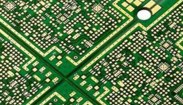
IC Substrate Definition and Function
IC Substrate Definition: A base board used to encapsulate bare IC chips.
IC Substrate Function
(1) Carrying semiconductor IC chips.
(2) The internal circuit is arranged for the connection between the chip and the circuit board.
(3) Protect, fix, support IC chip, provide heat dissipation channel, is the intermediate product of communication chip and PCB.

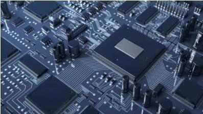
IC Packaging
IC Substrate born: in the mid-1990s, less than 20 years old. The advent of new integrated circuit (IC) high-density packaging forms, such as BGA (ball grid array packaging) and CSP (chip size packaging), has resulted in a necessary new carrier for packaging -- IC packaging substrate.
* Semiconductor development: valve - Transistor - Through hole assembly - surface Packaging (SMT) - Chip level Packaging (CSP, BGA) - System Packaging (SIP)
* PCB and semiconductor technology are interdependent, close, penetration, close coordination, PCB can achieve a variety of chips, components between the electrical insulation and electrical connection, to provide the required electrical characteristics.
Technical parameters Number of layers, 2 ~ 10 layers;
PCB board thickness, usually 0.1 ~ 1.5mm;
Minimum PCB board thickness tolerance *0 micron;
Minimum aperture, through hole 0.1mm, microhole 0.03mm;
* Minimum pattern width/spacing, 10~80 microns;
Minimum ring width, 50 microns;
* Contour tolerance, 0~50 micron;
* Buried blind hole, impedance, buried resistance capacity;
* Surface coating, Ni/Au, soft gold, hard gold, Nickel/palladium/gold, etc.
* Board size, ≤150*50mm (single IC carrier);
That is to say, THE IC Substrate requires more fine, high density, high number of feet, small volume, hole, disk, line smaller, ultra-thin core layer. Therefore, it is necessary to have precise interlayer alignment technology, pattern imaging technology, electroplating technology, drilling technology and surface treatment technology. Higher requirements have been put forward for product reliability, equipment and instruments, materials and production management. Therefore, the technical threshold of IC Substrate is high and the research and development is not easy.
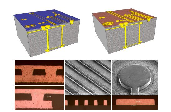
Technical difficulties Compared with traditional PCB manufacturing, the technical difficulties to be overcome for IC Substrate are as follows:
(1) core board production technology core board thin, easy to deformation, especially when the thickness of the plate ≤0.2mm, with plate structure, plate expansion and shrinkage, laminar parameters, interlayer positioning system and other technology needs to make a breakthrough, so as to achieve the ultra-thin core plate warping and pressing thickness of the effective control.
(2) Microporous technology
* Including: solder mask open process, laser drilling micro blind hole process, blind hole copper plating filling process.
* Conformalmask (Conformalmask) process is used to make reasonable compensation for laser blind hole window opening, and directly define the aperture and position of blind hole through the opened copper ring.
* Indicators involved in laser drilling microhole: hole shape, upper and lower aperture ratio, side erosion, glass fiber protruding, residual glue at the bottom of the hole, etc.
* Indicators involved in blind hole copper plating include: filling capacity, blind hole cavity, sag, copper plating reliability, etc.
* At present, the micropore size is 50~100 micron, and the number of layered pores reaches 3, 4 and 5 orders.
(3) Graphic formation and copper plating technology
Pattern compensation technology and control; Fine pattern production technology; Copper plating thickness uniformity control technology; Micro erosion control technology for fine pattern.
* The current pattern width spacing requirement is 20~50 microns. Copper plating thickness uniformity requirement is 18* micron, etching uniformity ≥90%.
(4) welding resistance process * including plug hole process, welding resistance printing technology, etc.
* The height difference between the solder resistance surface of the IC Substrate is less than 10 microns, and the height difference between the solder resistance and the pad surface is less than 15 microns.
(5) Surface treatment technology
* Uniformity of thickness of nickel/gold plating; Both soft and hard gold plating process on the same plate; Nickel/palladium/gold plating process.
* Lineable surface coating, selective surface treatment technology.
(6) Testing capability and product reliability testing technology
* Equipped with a number of testing equipment/instruments different from the traditional PCB factory.
* Master reliability testing techniques different from conventional ones.
(7) In general, the production of IC Substrate involving more than ten aspects of technology:
Graph dynamic compensation; Graphic electroplating process for thickness uniformity of copper plating; The whole process material expansion and shrinkage control; Surface treatment process, soft gold and hard gold selective electroplating, nickel/palladium/gold plating process;
* Core plate wafer production;
* High reliability detection technology; Microporous processing;
* If stacked micro 3, 4, 5, production process;
* Multiple laminated pressure; Laminate ≥4 times; Drilling ≥5 times; Electroplating ≥5 times.
* Wire pattern formation and etching;
* High precision alignment system;
* Welding stopper hole process, electroplating filling microhole process;
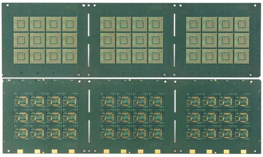
IC Substrate classification
By the form of encapsulation

Packaging Trend
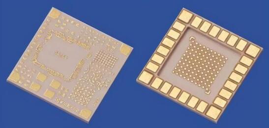
(1) BGA
*BallGridAiry, BGA, Spherical Array Package.
* This kind of package of the board heat dissipation, electrical performance is good, chip pin can be greatly increased, applied to 300 pin number (pincount) above IC package.
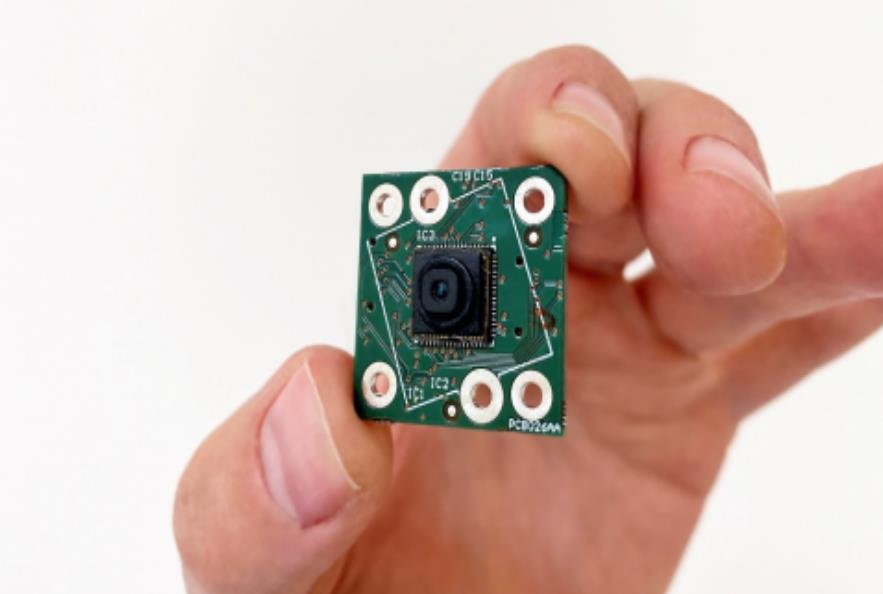
(2) CSP
*CSP, chipscalepackaging, chip level size packaging.
* Is a single chip package, light weight, small, its package size and IC itself size is almost the same or slightly larger, used in memory products, communication products, pin number is not high electronic products.
(3) coated crystal PCB board
* FlipChip (FC) is a type of package in which the front side of the chip is flipped (Flip) and the convex block is directly connected to the PCB.
This type of substrate has the advantages of low signal interference, low loss of connection circuit, good electrical performance, efficient heat dissipation and so on.
(4) Multi-chip module
* Multi-chip (MCM) module Multiple chips with different functions in the same package.
* This is the best solution for electronic products to light, thin, short, less than high-speed wireless. Used in high - order large computers or special performance electronic products.
* Because there are multiple chips in the same package, signal interference, heat dissipation, thin line design, and so on, there is no more complete solution, which belongs to the active development of products.
By material propertie
(1) Hard PCB board. sealing loading PCB
* Rigid organic packaging substrate made of epoxy, BT, ABF resin. Its output value is the majority of IC packaging substrate. CTE (coefficient of thermal expansion) ranges from 13 to 17ppm/ degree Celsius.
(2) Soft plate sealing loading PCB.
* The packaging substrate made of PI (polyimide), PE (polyester) resin flexible substrate, CTE is 13 ~ 27ppm/ degree Celsius.
(3) Ceramic substrate
* Aluminum oxide, aluminum nitride, silicon carbide and other ceramic materials as the packaging substrate. CTE is small, 6 ~ 8ppm/ degree Celsius.
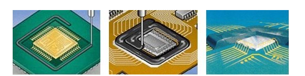
Distinguished by the technology of connection
(1) Play pattern to engage the carrier plate
* The gold wire connects the IC to the PCB.
(2) TAB PCB
*TAB -- TapeAutomatedBonding
* The inner pins of the chip are connected with the chip, and the outer pins are connected with the packaging board.
(3) Overlay crystal bonding PCB.
*Filpchip, the wafer is Filp bumped and directly connects to the IC Substrate.