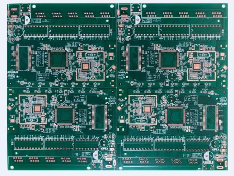
Radio frequency (RF) PCB board design is often described as a "black art" due to its theoretical uncertainty, but this view is only partially true, and there are many guidelines for RF circuit board design that can and should not be followed and neglected rule. However, when it comes to the actual design, the real trick is how to compromise these guidelines and laws when they cannot be implemented accurately due to various design constraints. Of course, there are many important RF design topics worth discussing, including impedance and impedance matching, insulation materials and laminates, and wavelengths and standing waves, but this article will focus on various issues related to RF board partition design. Today's cell phone designs integrate everything in a variety of ways, which is bad for RF board design. The industry is now very competitive, and everyone is looking for ways to integrate multiple functions with the size and cost. Analog, digital, and RF circuits are all tightly packed together with very little space to separate their respective problem areas, and the number of layers is often reduced due to cost considerations. It's amazing that a multipurpose chip can integrate multiple functions on a very small die, and the pins to connect to the outside world are arranged so closely together that the RF, IF, analog, and digital signals are very close together, But they are usually electrically irrelevant. Power distribution can be a nightmare for designers, with different parts of the circuit being time-shared as needed, with software-controlled switching in order to preserve battery life. This means you may need 5 or 6 working power sources for your cell phone.

RF Layout Concept
When designing an RF layout, there are several general principles that must be prioritized: isolate the high-power RF amplifier (HPA) from the low-noise amplifier (LNA) as much as possible, and in short, keep the high-power RF transmit circuit Keep away from low power RF receive circuits. You can easily do this if you have a lot of physical space on your PCB, but usually, with a lot of components and less space on the PCB, this is usually not possible. You can put them on both sides of the PCB board, or have them work alternately instead of simultaneously. High power circuits may also sometimes include RF buffers and voltage-controlled oscillators (VCOs). Make sure that there is at least one whole ground in the high-power area on the PCB without vias. Of course, the more copper, the better. Later, we will discuss how to break this design principle as needed, and how to avoid the problems that can arise from it. Chip and power supply decoupling is also extremely important, and several ways to implement this principle will be discussed later. The RF output usually needs to be kept away from the RF input, which we will discuss in detail later. Sensitive analog signals should be kept as far away as possible from high-speed digital and RF signals.
How to partition?
Design partitions can be broken down into physical and electrical partitions. Physical partitions mainly involve issues such as component placement, orientation, and shielding; electrical partitions can continue to be broken down into partitions for power distribution, RF traces, sensitive circuits and signals, and grounding. First we discuss the physical partition problem. Component placement is the key to implementing an RF design. An effective technique is to first fix the components located on the RF path and adjust their orientation to minimize the length of the RF path, keep the input away from the output, and separate the components as far as possible. power circuits and low power circuits. An effective board stacking method is to arrange the main ground plane (main ground) on the second layer below the surface layer and run the RF lines on the surface layer as much as possible. Reducing the via size on the RF path not only reduces the path inductance but also reduces ghost solder joints on the main ground and reduces the chance of RF energy leaking to other areas within the stack. In physical space, linear circuits like multistage amplifiers are usually sufficient to isolate multiple RF zones from each other, but duplexers, mixers, and IF amplifiers/mixers always have multiple RF/IFs The signals interfere with each other, so care must be taken to minimize this effect. The RF and IF traces should be crossed as much as possible, with a ground space between them as much as possible. Proper RF routing is very important to the performance of the entire PCB, which is why component placement often takes up most of the time in cellular phone PCB design. On a cellular phone PCB, it is often possible to place the LNA circuit on one side of the PCB and the high power amplifier on the other side, and finally connect them to the RF side and baseband processing on the same site through a duplexer on the antenna of the device. Some tricks are required to ensure that straight-through vias do not transfer RF energy from one side of the board to the other, and a common technique is to use blind vias on both sides. The detrimental effects of straight-through vias can be minimized by arranging the straight-through vias in areas where both sides of the PCB are free from RF interference.
Sometimes it is not possible to ensure sufficient isolation between multiple circuit blocks, in which case metal shields must be considered to shield RF energy in the RF area, but metal shields also have problems, such as their own cost and Assembly costs are very expensive; metal shields with irregular shapes are difficult to ensure high precision during manufacture and rectangular or square metal shields limit the layout of components; metal shields are not conducive to component replacement and fault location; due to The metal shield must be soldered to the ground and must be kept at an appropriate distance from the components, thus taking up valuable PCB board space. It is very important to ensure the integrity of the shielding cover as much as possible. The digital signal lines entering the metal shielding cover should go to the inner layer as much as possible, and the PCB board below the wiring layer is the ground layer. The RF signal line can go out from the small gap at the bottom of the metal shield and the wiring layer at the ground gap, but as much ground as possible should be distributed around the gap, and the ground on different layers can be connected together through multiple vias. Despite the above problems, metal shields are very effective and often the solution for isolating critical circuits. In addition, proper and effective decoupling of chip power supply is also very important. Many RF chips with integrated linear lines are very sensitive to power supply noise, typically requiring up to four capacitors and an isolation inductor per chip to ensure all power supply noise is filtered).
The value of the capacitor is usually determined by its self-resonant frequency and low lead inductance, and the value of C4 is chosen accordingly. The values of C3 and C2 are relatively large due to their own pin inductance, so the RF decoupling effect is less, but they are more suitable for filtering lower frequency noise signals. Inductor L1 prevents RF signals from coupling into the chip from the power lines. Remember: all traces are a potential antenna that can both receive and transmit RF signals, and it is also necessary to isolate induced RF signals from critical wiring. The physical location of these decoupling components is also often critical. The layout principles for these important components are: C4 should be as close as possible to the IC pin and grounded, C3 must be close to C4, C2 must be close to C3, and the IC pin must be close to C4. The connection traces should be as short as possible, and the ground terminals of these components (especially C4) should usually be connected to the ground pins of the chip through the next ground plane. The vias connecting the components to the ground layer should be as close as possible to the component pads on the PCB. Blind holes on the pads are used to reduce the inductance of the connection line, and the inductance should be close to C1. An integrated circuit or amplifier often has an open-drain output, so a pull-up inductor is required to provide a high-impedance RF load and a low-impedance DC source. The same principle applies to decoupling the supply on this inductor side. Some chips require multiple power supplies to operate, so you may need two or three sets of capacitors and inductors to decouple them separately, which can cause some trouble if there isn't enough space around the chip. Remember that inductors are rarely close together in parallel, as this will form an air core transformer and induce interfering signals, so they must be at least as far apart as one of the devices is high, or at right angles to reduce their mutual inductance arrive.
The principles of electrical partitioning are generally the same as physical partitioning, but there are a few other factors involved. Certain parts of modern cellular phones operate at different voltages and are controlled by software to extend battery life. This means that cell phones need to run multiple power sources, which creates more problems with isolation. Power is usually brought in at the connector and is immediately decoupled to filter out any noise from outside the board before being distributed through a set of switches or voltage regulators. Most circuits in cell phones have fairly small DC currents, so trace width is usually not an issue, however, a separate high-current trace as wide as possible must be run for the power supply of the high-power amplifier to minimize the transmission voltage drop. To avoid too much current loss, multiple vias are needed to pass current from one layer to another. Additionally, if the high power amplifier is not sufficiently decoupled at its power supply pins, high power noise will radiate across the board and cause various problems. Grounding of high-power amplifiers is critical and often requires a metal shield. In most cases, it is also critical to ensure that the RF output is kept away from the RF input. This also applies to amplifiers, buffers, and filters. In the worst case, amplifiers and buffers have the potential to self-oscillate if their outputs are fed back to their inputs with the proper phase and amplitude. In any case, they will work stably under any temperature and voltage conditions. In fact, they can become unstable and add noise and intermodulation signals to the RF signal.
If the RF signal lines have to be looped back from the input of the filter to the output, this can seriously damage the bandpass characteristics of the filter. In order to obtain good isolation between input and output, first, a ground must be placed around the filter, and secondly, the ground should be placed in the lower area of the filter and connected to the main ground around the filter. It is also a good idea to keep the signal lines that need to go through the filter as far away from the filter pins as possible. Also, be very careful about grounding everywhere on the board, or you could unknowingly introduce a coupling channel that you don't want to happen. Figure 3 details this grounding approach. Sometimes single-ended or balanced RF signal lines can be chosen, and the same principles regarding cross-interference and EMC/EMI apply here. Balanced RF signal lines can reduce noise and cross-interference if they are routed correctly, but their impedance is usually high, and a reasonable line width should be maintained to obtain an impedance that matches the source, trace, and load. Actual wiring may There will be difficult. A buffer can be used to improve isolation because it can split the same signal into two parts and use it to drive different circuits, especially if the LO may need a buffer to drive multiple mixers. When the mixer reaches common mode isolation at RF frequencies, it will not function properly. Buffers are good at isolating impedance changes at different frequencies so that circuits do not interfere with each other. Buffers are a great help in the design, they can be placed right after the circuit that needs to be driven, so that the high power output traces are very short, because the input signal level of the buffer is relatively low, so they are not easy to be affected by other circuits on the board. circuit causing interference. There are also many very sensitive signal and control lines that require special attention, but they are beyond the scope of this article, so they are only briefly discussed here and will not be described in detail.
Voltage Controlled Oscillators (VCOs) convert changing voltages to changing frequencies, a feature used for high-speed channel switching, but they also convert small amounts of noise on the control voltage into small frequency changes, which give RF signals add noise. In general, after this, you can no longer remove noise from the RF output signal. So where is the difficulty? First, the desired bandwidth of the control line may range from DC to 2MHz, and filtering to remove noise in such a wide band is almost impossible; second, the VCO control line is usually part of a feedback loop that controls the frequency, which is in many Noise can be introduced everywhere, so the VCO control lines must be handled with great care. Make sure that the ground below the RF traces is solid and that all components are firmly connected to the main ground and isolated from other traces that may introduce noise. In addition, make sure that the power supply of the VCO is adequately decoupled, since the RF output of the VCO tends to be at a relatively high level, the VCO output signal can easily interfere with other circuits, so special attention must be paid to the VCO. In fact, the VCO is often placed at the end of the RF area, and sometimes it requires a metal shield.
The resonant circuit (one for the transmitter and the other for the receiver) is related to the VCO but also has its own characteristics. Simply put, a resonant circuit is a parallel resonant circuit with a capacitive diode that helps set the VCO operating frequency and modulate speech or data onto an RF signal. All VCO design principles apply equally to resonant circuits. Resonant circuits are often very sensitive to noise due to their considerable number of components, wide distribution on the board, and typically operating at a very high RF frequency. Signals are usually arranged on adjacent pins of the chip, but these signal pins need to work with relatively large inductors and capacitors, which in turn requires these inductors and capacitors to be located close together and connected back to a noise-sensitive control loop. It is not easy to do this. The automatic gain control (AGC) amplifier is also a problem-prone place, and there will be an AGC amplifier in both the transmit and receive circuits. AGC amplifiers are generally effective at filtering out the noise, but the ability of cellular phones to handle rapid changes in transmitted and received signal strength requires the AGC circuit to have a fairly wide bandwidth, which makes AGC amplifiers on some critical circuits easy to introduce noise. Good analog circuit design techniques must be followed when designing AGC lines, and this has to do with very short op-amp input pins and very short feedback paths, both of which must be kept away from RF, IF, or high-speed digital signal traces. Also, good grounding is essential, and the power supply to the chip must be well decoupled. If you have to run a long wire at the input or output, it's at the output, which usually has a much lower impedance and is less prone to inductive noise. Usually the higher the signal level, the easier it is to introduce noise into other circuits. In all PCB design, it is a general principle to keep digital circuits away from analog circuits as much as possible, and it also applies to RF PCB design. The common analog ground is usually as important as the ground used to shield and separate the signal lines, the problem is that it is very little you can do in this regard each time without foresight and careful planning. Careful planning, thoughtful component placement, and thorough placement evaluation are therefore very important in the early stages of design, as inadvertent design changes can result in a near-finished design having to be rebuilt. This serious consequence of negligence is not a good thing for your personal career development anyway. Also, keep the RF lines away from analog lines and some very critical digital signals. All RF traces, pads, and components should be filled with ground copper as much as possible and connected to the main ground as much as possible. Micro-via build boards like breadboards are useful in the RF circuit development stage, if you choose build boards, you can use as many vias as you want without any expense, otherwise drilling holes in a normal PCB will increase development cost, which increases costs when mass-produced.
If the RF traces must pass through the signal lines, try to route a layer of ground connected to the main ground along the RF traces between them. If not possible, make sure they are crisscrossed to minimize capacitive coupling, and as much ground as possible around each RF trace, and connect them to the main ground. Also, reducing the distance between parallel RF traces can reduce inductive coupling. A solid monolithic ground plane placed directly under the surface layer, the isolation effect, although a little careful design other practices also work. I've tried splitting the ground plane into pieces to isolate the analog, digital, and RF lines, but I've never been satisfied with the results because there will always be some high-speed signal lines going through these separate grounds, it's not a piece of a good thing. On each layer of the PCB board, lay as many grounds as possible and connect them to the main ground. Place the traces as close together as possible to increase the number of pads on the internal signal and power distribution layers, and adjust the traces so that you can route ground connection vias to isolated pads on the surface. Free grounds on various layers of the PCB board should be avoided as they can pick up or inject noise like a small antenna.