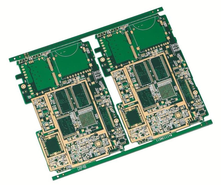
For those who study electronics with fr4 pcb, it is natural to set test points on circuit boards, but for those who study mechanics, what is the test point?
Basically, the purpose of setting test points is to test whether the components on the circuit board meet the specifications and solderability. For example, if you want to check whether the resistance on a circuit board is faulty, the simplest way is to measure its two ends with a multimeter. However, there is no way for you to use an electric meter to slowly measure whether each resistance, capacitance, inductance, and even IC circuit on each board is correct in a mass-produced factory, so there is the so-called ICT (In-Circuit-Test) automatic test machine, which uses multiple probes (commonly referred to as "Bed-Of-Nails" fixture) to simultaneously contact all parts and circuits on the board that need to be measured, Then the characteristics of these electronic parts are measured in sequence by means of program control with sequence as the main part and parallel as the auxiliary part. Generally, it takes only 1 to 2 minutes to test all parts of the general board. Depending on the number of parts on the circuit board, the more parts, the longer the time. However, if these probes are allowed to directly contact the electronic parts on the board or their welding feet, it is likely to destroy some electronic parts, which is counterproductive. So the smart engineer invented the test point, which leads out a pair of circular small points at both ends of the part. There is no mask on the upper surface, so that the test probe can contact these small points instead of directly contacting the measured electronic parts.

In the early days when the traditional plug-in (DIP) was still used on the circuit board, it was true that the solder leg of the part would be used as the test point, because the solder leg of the traditional part was strong enough to be needled, but the misjudgment of poor contact of the probe often occurred, because a residual film of solder paste flux would usually form on the surface of the solder of the common electronic parts after wave soldering or SMT eating tin, The impedance of this film is very high, which often leads to poor contact of the probe. Therefore, at that time, it is often seen that the test operators of the production line often blow hard with the air gun, or wipe the places that need to be tested with alcohol.
In fact, there will also be poor contact of the probe at the test point after wave soldering. Later, after the prevalence of SMT, the situation of test misjudgment has been greatly improved, and the application of test points has also been greatly entrusted with heavy responsibilities, because the parts of SMT are usually fragile and can not bear the direct contact pressure of the test probe, so the use of test points can avoid the probe directly touching the parts and their welding feet, which not only protects the parts from damage, but also indirectly greatly improves the reliability of the test, because the number of misjudgment is reduced. However, with the development of science and technology, the size of the circuit board is getting smaller and smaller. It is difficult to squeeze so many electronic parts on the small circuit board. Therefore, the problem of test points occupying the space of the circuit board is often a tug of war between the design end and the manufacturing end. However, this issue will be discussed later when we have the opportunity. The appearance of the test point is usually round, because the probe is also round, which is easier to produce, and it is easier to make adjacent probes close to each other, so as to increase the needle planting density of the needle bed.
1. There are some institutional limitations when using a needle bed for circuit testing. For example, the minimum diameter of the probe has a certain limit, and the needle with too small diameter is easy to break and damage.
2. The distance between pins is also limited, because each pin must come out of a hole, and the back end of each pin must be welded with a flat cable. If the adjacent holes are too small, in addition to the problem of contact short circuit between pins, the interference of flat cable is also a big problem.
3. Needles cannot be planted beside some high parts. If the probe is too close to the high part, there will be a risk of damage caused by collision with the high part. In addition, because the part is high, it is usually necessary to open a hole on the needle bed of the test fixture to avoid it, which also indirectly leads to the failure of needle implantation. Test points for all parts on the circuit board that are increasingly difficult to accommodate.
4. As the board is getting smaller and smaller, the number of test points has been discussed repeatedly. Now there are some methods to reduce test points, such as Net test, Test Jet, Boundary Scan, JTAG, etc; There are also other test methods that want to replace the original needle bed test, such as AOI and X-Ray, but at present each test does not seem to be able to replace ICT 100%.
As for the needle planting ability of ICT, we should ask the matching fixture manufacturer, that is, the minimum diameter of the test point and the minimum distance between the adjacent test points. Usually, there will be a desired minimum value and the minimum value that can be reached. However, the manufacturer with scale will require that the distance between the minimum test point and the minimum test point should not exceed how many points, otherwise the fixture is also vulnerable to damage fr4 pcb.