Language
Get quotes quickly.
sales@ipcb.com
2022-05-11
In low-speed PCB board where the concept of network is widely used on high-speed circuit PCBs, "ground" is also popular, and "ground" itself is a network.
2022-05-09
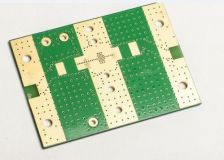
Ground bounce of high-speed circuit PCB board.
Most PCB boards contain some functional subsystems or areas, each functional subsystem consists of a set of devices and their supporting circuits.
2022-05-06
In a high-speed PCB board system, the impedance mismatch on the transmission line will cause signal reflection, and signal distortion such as overshoot, undershoot and ringing will occur.
For the noise on the PCB board, when it is found that electromagnetic interference occurs in the digital circuit, the main reason is that the obvious noise voltage can be observed on the power line and the ground line with an oscilloscope.
2022-05-05
The main purpose of the electromagnetic compatibility design of the PCB board is to reduce the electromagnetic radiation of the circuit board and ensure that the equipment meets the relevant standards.
The design of the mixed-signal circuit PCB board is very complicated.
2022-04-29
The role and characteristics of nickel electroplating process on PCB board.
About the operation process of PCB board light painting.
2022-04-28
Use multi-layer PCB board as much as possible.
When conducting PCB board wiring, it often happens that when the traces pass through a certain area.
2022-04-27
For PCB board technology MSD storage considerations, usually, after the material is removed from the placement machine.
The solution of PCB board mounting SMD on FPC,According to the placement accuracy requirements and the different types and quantities of components.
2022-04-26
Principles of PCB board layout Operation Skills,Filter Capacitors, Decoupling Capacitors, Bypass Capacitors,Reasons for Paralleling a Small Capacitor to a Large Capacitor.
On PCB board,for simultaneous switching noise analysis of FPGAs, today's CMOS technology allows a single FPGA device to have multiple I/O interfaces.
2022-04-25
The following checklist covers all aspects of the design cycle, with additional items for special: applications. General PCB board design drawing inspection items.
The overall layout of the printed circuit boards and device layout.
2022-04-22
The preferred process route has been determined, and all devices have been placed on the PCB board.
It introduces the application of PCB board design tools to solve these problems, such as skin effect and dielectric loss, the effect of vias and connectors.
2022-04-21
The printed circuit boards industry is shifting the surface treatment from hot air leveled tin spray (tin-lead eutectic) to other surface treatments.