Anti-deformation installation of printed circuit board components
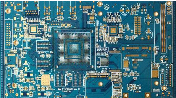
1. During the installation of the reinforced frame and PCBA, and the installation of PCBA and the chassis, the warped PCBA or warped reinforced frame is directly or forcibly installed and the PCBA is installed in the deformed chassis. Installation stress causes damage and fracture of component leads (especially high-density ICs such as BGS, surface mount components), relay holes of multilayer PCBs, and inner connecting wires and pads of multilayer PCBs
For PCBA or reinforced frame whose warpage does not meet the requirements, the designer should cooperate with the craftsman to take or design effective "pad" measures at the bow (twist) part before installation.

2. Analysis
Among chip resistor-capacitor components, ceramic chip capacitors have the highest probability of defects, mainly as follows:
PCBA bowing and deformation caused by wiring harness installation stress.
PCBA flatness after welding is greater than 0.75%.
The design of the pads at both ends of the ceramic chip capacitor is asymmetrical.
Common pad, the welding time is greater than 2s, the welding temperature is higher than 245 degree Celsius, and the total number of welding exceeds the specified value 6 times.
The coefficient of thermal expansion is different between ceramic chip capacitors and PCB materials.
When the PCB is designed, the distance between the fixing hole and the ceramic chip capacitor is too close to cause stress during tightening.
Even if the pad size of the ceramic chip capacitors on the PCB is the same, if the amount of solder is too much, it will increase the tensile stress on the chip capacitor when the PCB is bent; the correct amount of solder should be 1 of the height of the solder terminal of the chip capacitor /2~2/3
Any external mechanical or thermal stress will cause cracks in the ceramic chip capacitors.
Cracks caused by the extrusion of the pick-and-place head will show up on the surface of the components. They are usually circular or half-moon-shaped cracks with a changed color, located at or near the center of the capacitor.
Cracks caused by incorrect setting of placement machine parameters. The pick and place head of the placement machine uses a vacuum pipette or center clamp to position the components. Excessive Z-axis downward pressure will break the ceramic components. If the pick-and-place head of the placement machine applies a large enough force to a certain position other than the central area of the ceramic body, the stress applied to the capacitor may be large enough to damage the components.
Inappropriate selection of the size of the pick and place head will cause cracks. The small-diameter patch pick-and-place head will concentrate the placement force when patching, so that the smaller ceramic chip capacitor area can withstand greater pressure, causing cracks in the ceramic chip capacitor.
Inconsistent amount of solder will produce inconsistent stress distribution on the components, and stress concentration at one end will cause cracks.
The root causes of cracks are the porosity and cracks between the layers of the ceramic chip capacitor and the ceramic chip.
3. Solution:
Strengthen the screening of ceramic chip capacitors: Use C-SAM and SLAM to screen ceramic chip capacitors to screen out defective ceramic capacitors.