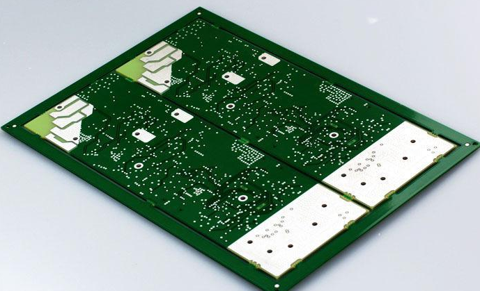
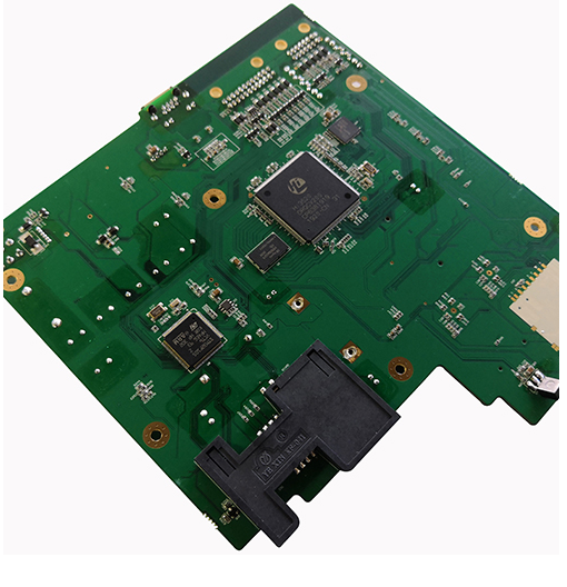
Analysis on the assembly process of LGA in PCBA processing
What I shared today is an analysis of the assembly process of LGA in PCBA processing. In addition to the common components in PCBA processing, we will also see special components, such as chips, LGA. Today we are talking about the protagonist of PCBA processing LGA, the assembly process of LGA is analyzed.
1. Background
LGA, that is, no solder ball array package, similar to BGA, but without solder balls.

2. Process characteristics
For bottom surface-end packages, the stand-off between the bottom of the package and the PCB surface after soldering is very small, generally only 15-25um, and the flux residues will often bridge. At the same time, the solvent in the flux for PCB patch processing is generally not easy to volatilize, forming a viscous shape instead of a general solid. Since most of the solvents in the flux use alcoholic organic compounds, which have hydrophilic characteristics, if there is a bias voltage between adjacent pads, it may leak.
3. Assembly process
Generally, the center-to-center distance of the LGA pads is relatively large, and the 1.27mm design is mostly adopted. The key to the Smt soldering process is to ensure that the flux activator is completely volatilized and decomposed. Therefore, a longer preheating time, a higher soldering peak temperature, and a longer soldering time should be used.
Long heating time: designed to completely volatilize the solvent in the flux.
High welding peak temperature and long welding time: aiming to make the activator decompose completely or volatilize completely.
4. Design
It is recommended to use solder mask to define the pad design, which helps to ensure the separation of the solder around the LGA pad.
The above is some analysis of the assembly process of LGA in PCBA processing, I hope it will be helpful to you. If you need PCBA processing business or SMT processing business, please contact us, we will do our best to serve you, thank you.
iPCB is happy to be your business partner. Our business goal is to become the most professional prototyping PCB manufacturer in the world. With more than ten years of experience in this field, we are committed to meeting the needs of customers from different industries in terms of quality, delivery, cost-effectiveness and any other demanding requirements. As one of the most experienced PCB manufacturers and SMT assemblers in China, we are proud to be your best business partner and good friend in all aspects of your PCB needs. We strive to make your research and development work easy and worry-free.
quality assurance
iPCB has passed ISO9001:2008, ISO14001, UL, CQC and other quality management system certifications, and produces standardized and qualified PCB products. We master complex process skills and use professional equipment such as AOI and Flying Probe to control production, X-ray inspection machines, etc. . Finally, we will use double FQC inspection of appearance to ensure shipment under IPC II standard or IPC III standard.