Why are PCBA multi-layer boardsnot odd-numbered layers but all even-numbered layers?
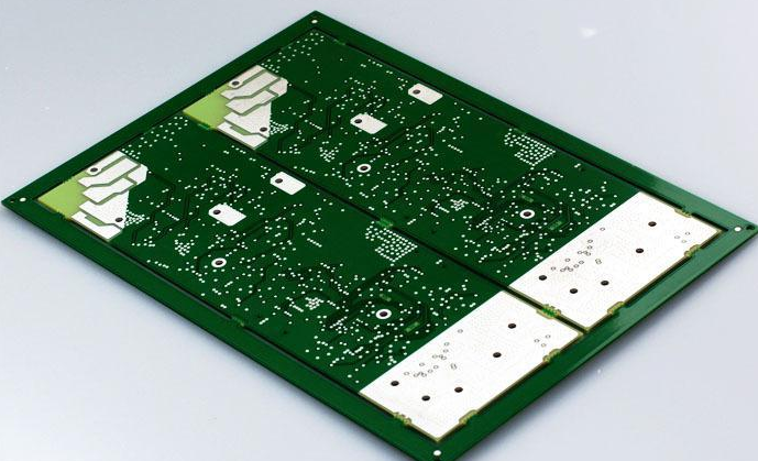
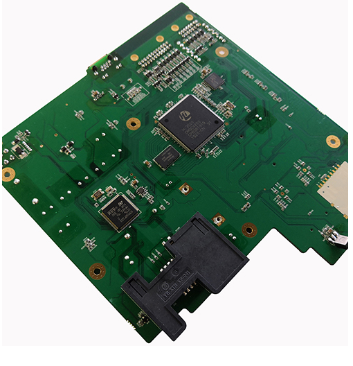
There are single-sided, double-sided and multi-layer PCBA boards. The number of multi-layer boards is not limited. There are currently more than 100 layers of PCBA, and common multi-layer PCBAs are four-layer and six-layer boards. So why do people have the question "Why are PCBA multilayer boards all even-numbered layers?"? Relatively speaking, PCBAs with even-numbered layers do have more advantages than PCBAs with odd-numbered layers.
01, lower cost
Because of the lack of a layer of dielectric and foil, the raw material cost of odd-numbered PCBA boards is slightly lower than that of even-numbered PCBA. However, the processing cost of odd-numbered layer PCBA is significantly higher than that of even-numbered layer PCBA. The processing cost of the inner layer is the same, but the foil/core structure obviously increases the processing cost of the outer layer.
Odd-numbered layer PCBA needs to add a non-standard laminated core layer bonding process on the basis of the core structure process. Compared with the nuclear structure, the production efficiency of factories that add foil to the nuclear structure will decrease. Before lamination and bonding, the outer core requires additional processing, which increases the risk of scratches and etch errors on the outer layer.

02, balance structure to avoid bending
The best reason not to design PCBA with odd-numbered layers is that the odd-numbered layer circuit boards are easy to bend. When the PCBA is cooled after the multi-layer circuit bonding process, the different lamination tension of the core structure and the foil-clad structure will cause the PCBA to bend. As the thickness of the circuit board increases, the risk of bending of the composite PCBA with two different structures increases. The key to eliminating circuit board bending is to use a balanced stack. Although a certain degree of bending of the PCBA meets the specification requirements, the subsequent processing efficiency will be reduced, resulting in an increase in cost. Because special equipment and craftsmanship are required during assembly, the accuracy of component placement is reduced, which will damage the quality.
To put it another way, it’s easier to understand: In the PCBA process, the four-layer board is better controlled than the three-layer board, mainly in terms of symmetry. The warpage of the four-layer board can be controlled below 0.7% (IPC600 standard), but When the size of the three-layer board is large, the warpage will exceed this standard, which will affect the reliability of the SMT patch and the entire product. Therefore, the general designer does not design an odd-numbered layer board, even if the odd-numbered layer realizes the function, it will It is designed as a fake even-numbered layer, that is, 5 layers are designed into 6 layers, and 7 layers are designed into 8-layer boards.
Based on the above reasons, PCBA multi-layer boards are mostly designed with even-numbered layers and fewer odd-numbered layers.
How to balance the stacking and reduce the cost of odd-numbered PCBA?
What should I do if an odd-numbered PCBA appears in the design? The following methods can be used to achieve balanced stacking, reduce PCBA production costs, and avoid PCBA bending.
1) A signal layer and use it.
This method can be used if the power layer of the PCBA is designed to be an even number and the signal layer is an odd number. The added layer does not increase the cost, but it can shorten the delivery time and improve the quality of PCBA.
2) Add an additional power layer.
This method can be used if the power layer of the PCBA is designed to be odd and the signal layer is even. A simple method is to add a layer in the middle of the stack without changing other settings. First, follow the odd-numbered PCBA type wiring, then copy the ground layer in the middle, and mark the remaining layers. This is the same as the electrical characteristics of a thickened layer of foil.
3) Add a blank signal layer near the center of the PCBA stack.
This method minimizes the stacking imbalance and improves the quality of PCBA. First, follow the odd-numbered layers to route, then add a blank signal layer, and mark the remaining layers. Used in microwave circuits and mixed media (different dielectric constants) circuits.