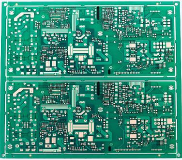
The performance requirements of PCB circuit boards are not as strict as they are now.
There are fewer materials used to make PCBs.
PCB design tools do not have the complicated board stacking and configuration functions as they do today.
Fortunately, since most major design tools are equipped with advanced PCB layer configuration capabilities, this part of the PCB layout process is now very different. Having said that, designers still have the responsibility to complete the process of configuring the correct layer stack for their design. We will study this process and discuss some ideas for building and configuring a layer stack in PCB design software.
The number of layers on a printed circuit board is directly related to the number of nets that need to be wired. As the demand for PCB circuits increases, so does the number of components, and ultimately the number of networks also increases. At the same time, the complexity and pin count of active components are also increasing, which increases the net number on the circuit board. The answer to these increases is to reduce the trace width or increase the number of layers of the board, or both, which unfortunately leads to higher manufacturing costs.

Although the average number of components on the PCB and the net number have increased, the electrical performance indicators of the circuit board have also improved. Designers quickly discovered that although wiring used to require four-layer boards to require six layers, in fact they must reach eight layers to obtain the required electrical performance. Some reasons for these additional layers include:
1. There is more room for isolation control impedance routing.
2. Differential pair routing is restricted to as few layers as possible.
3. Microstrip line and strip line layer stacking configuration.
4. Additional plane layer for multiple power and grounding grids.
With the continuous development of circuit board functions, another factor has been introduced in the process of creating the circuit board layer stack. Compared with previously used circuit boards, the higher operating speeds of current circuit boards may require more advanced circuit board manufacturing materials. The same is true for high-power boards or boards that will be used in harsh environments. These materials may change the transmission line characteristics of the circuit originally calculated for the standard FR-4 material, which in turn may require changes to the layer stack configuration.
For today's advanced electronic equipment, it is crucial to create the correct stack of layers to ensure that the boards will operate at their high performance.
tool:
If the PCB design tools are not good enough, they cannot be used effectively when creating PCB stackups. This not only slows down the work speed and increases the frustration of the work, but also may affect the design level of the circuit board.
PCB CAD tools can do many things to help layout designers create and configure circuit board layer stacks. The first is to merge the automatic generator or wizard, as shown in the figure above. These tools allow designers to specify the number of layers and configurations of the stack, and these tools require extensive creation in the database. The next step is to give the designer full control over the details of the layer stack, including the ability to specify conductive and dielectric board materials. Designers should be able to specify values and tolerances, and configure how layers should be laid out when setting layout parameters.