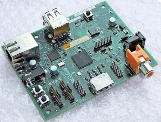
With the development of electronic products towards miniaturization and thinning, surface mount technology (SMT) SMT chip processing emerged at the historic moment and has become the mainstream of current electronic production. This chapter will introduce the process flow of SMT chip processing, the installation of components and production equipment, the repair of SMT circuit boards, and the application of micro assembly technology (MPT) on this basis.
Surface mount technology SMT patch is a fourth-generation electronic product installation technology that integrates surface electronic components, assembly equipment, auxiliary materials and soldering methods.
1. The development of surface mount technology (SMT patch)
Surface mounting technology has gone through the following four development stages from its emergence to the present:
The main technical goal of the first stage (1970-1985) was to apply miniaturized chip components to hybrid circuits.
In the second stage (1976-1985), in this stage, surface mounting technology enabled the development of electronic products toward multi-function and miniaturization, and at the same time promoted the development of surface mounting equipment, laying a foundation for the development of surface mounting technology.
In the third stage (1986-1995), screen printing and reflow soldering technologies were applied during this stage, resulting in lower product costs and higher cost performance.

The fourth stage (1996 to present) mass production of large-capacity, multi-functional, high-reliability, multi-layer and three-dimensional micro-chip components, the production equipment has a higher degree of automation and faster speed. Welding is developing towards lead-free environmental protection, and flip-chip welding and special welding have begun to be used.
Second, the characteristics of surface mount technology (SMT patch)
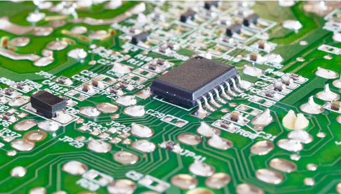
1. Realize miniaturization
On the electrodes of SMT components, some welding ends have no leads at all, and some have very short leads; the distance between adjacent electrodes is much smaller than that of traditional dual in-line integrated circuits (2.54mm). At present, the smallest pin center spacing has reached 0.3mm. In the case of the same degree of integration, the volume of SMT components is 60% to 90% smaller than traditional THT components, and the weight is also reduced by 60% to 90%.
2. Electrical performance is greatly improved
Surface mount components reduce parasitic leads and conductor inductance, while improving the characteristics of capacitors, resistors and other components. The transmission delay is small, the signal transmission speed is accelerated, and the radio frequency interference is eliminated at the same time, so that the high-frequency characteristics of the circuit are better, the working speed is faster, and the noise is significantly reduced.
3. Easy to realize automation, high-volume, high-efficiency production
Due to the standardization, serialization, and consistency of welding conditions of chip components, and the continuous birth of advanced high-speed placement machines, the automation of surface mounting is very high, and the production efficiency is greatly improved. For example, all types of new placement machines generally use advanced technologies such as "laser alignment" and "flight alignment detection".
4. Material costs and production costs are generally reduced
Because the volume of SMT components is generally reduced, the consumption of packaging materials for the components is reduced, and because of the high degree of production automation and the increase in yield, the selling price of SMT components is lower. And in SMT assembly, the components do not need to be pre-shaped or cut feet, and the printed circuit board does not need to be punched, which greatly saves manpower and material resources, so the production cost is generally reduced.
5. Product quality improvement
Due to the small size and strong function of chip integrated circuits, one chip integrated circuit on the SMT circuit board can realize the functions of several integrated circuits of the THT circuit, so the probability of failure of the circuit board is greatly reduced, and the work is more reliable and stable.
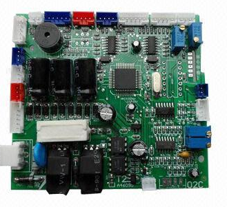
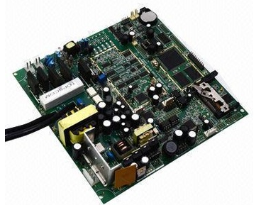
Third, the process flow of surface mount technology (SMT patch)
1. Assembly process flow of single-sided SMT circuit board
(1) Paste application process The paste application process is located at the forefront of the SMT production line. Its function is to apply the solder paste on the pads of the SMT circuit board to prepare for the mounting and soldering of the components.
(2) Mounting The surface mount components are accurately mounted on the fixed position of the SMT circuit board.
(3) Curing. Its function is to melt the patch glue, so that the surface mount components and the circuit board are firmly bonded together.
(4) Reflow soldering Its function is to melt the solder paste, so that the surface mount components and the PCB board are firmly bonded together.
(5) Cleaning Its function is to remove the solder residue (such as flux, etc.) harmful to the human body on the assembled circuit board.
(6) Inspection Its function is to inspect the welding quality and assembly quality of the assembled circuit board.
(7) Rework The function is to rework the circuit boards that have detected faults.
2. Assembly process flow of double-sided SMT circuit board
Perform reflow soldering on the A side of the printed circuit board first, and arrange a testing process to pick out the unqualified circuit boards for repair. Then reflow, clean and repair the B side of the printed circuit board.
3. Double-sided SMT+THT mixed assembly (double-sided reflow soldering, wave soldering) process
A surface coating paste-component placement-reflow soldering-flip board-B side red glue-component placement-glue curing-flip board-A side plug-in-pin bending --Wave soldering--Cleaning--Inspection--Rework
Double-sided hybrid assembly PCB boards have conductive layers on both sides (ie double-sided boards). Mount the chip integrated circuit on the A side of the PCB board with small pin spacing or SMT devices whose pins are at the bottom of the integrated circuit. Use reflow soldering. For mixed-insertion THT components, SMT components with large pin spacing and moderate weight on the B side are often wave soldered. However, with the improvement of reflow soldering technology, reflow soldering is now also useful. In order to reduce the damage to the solder joints of the A side that has been soldered during reflow soldering, the B side must use low temperature and low melting point solder paste. This mixed assembly process is suitable for PCB boards with high component density, components must be arranged on the bottom surface and more THT components. It can not only improve the processing efficiency, but also reduce the manual welding workload.