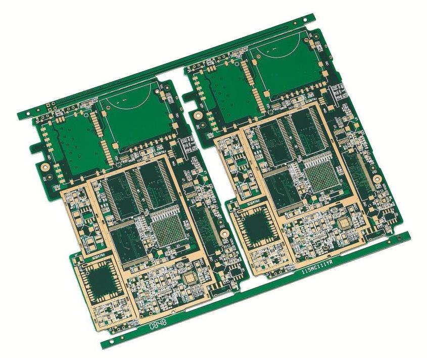
The characteristics of high-speed DSP system PCB board and several issues that should be paid attention to in reliability design, including power supply design, software and hardware anti-jamming design, electromagnetic compatibility design, heat dissipation design, and the wiring method of important signal lines of high-speed circuits, make each design more efficient. Reasonable and easy to implement. Due to the rapid development of microelectronics technology, the digital electronic system composed of IC chips is developing rapidly in the direction of large scale, small volume, and high speed, and the development speed is getting faster and faster. The application of new devices leads to high circuit layout density in modern EDA design, and the frequency of signals is also very high. With the use of high-speed devices, there will be more and more high-speed DSP (digital signal processing) system designs. The signal problem becomes a significant issue in designs that are characterized by ever-increasing system data rates, clock rates, and circuit densities, and whose PCB are designed to exhibit very different behavior than low-speed designs characteristics, that is, signal integrity problems, interference aggravation problems, electromagnetic compatibility problems, and so on. These problems can cause or directly bring about signal distortion, timing errors, incorrect data, address, and control lines, system errors and even system crashes. If they are not solved properly, they will seriously affect system performance and bring immeasurable losses. The solution to these problems mainly depends on circuit design. Therefore, the design quality of the PCB board is very important, and it is the only way to turn the design concept into reality. The following discusses several issues that should be paid attention to in PCB board reliability design in high-speed DSP systems.

Power Design
The first thing to consider when designing a high-speed DSP system PCB board is the power supply design. In power supply design, the following methods are commonly used to solve signal integrity problems.
Consider power and ground decoupling
With the increase in DSP operating frequency, DSP and other IC components tend to be miniaturized and packaged densely. Usually, multi-layer boards are considered in circuit design. It is recommended that a dedicated layer can be used for both power supply and ground. For example, the I/O power supply voltage of DSP is different from the core power supply voltage, so two different power supply layers can be used. If considering the high processing cost of multi-layer boards, a special layer can be used for the power supply with more wiring or relatively critical power supply, and other power supply layers can be used. The power supply can be routed in the same way as the signal lines, but pay attention to the width of the lines. Regardless of whether the circuit board has a special ground layer and power supply layer, a certain and reasonably distributed capacitance must be added between the power supply and the ground. In order to save space and reduce the number of through holes, it is recommended to use more chip capacitors. The chip capacitor can be placed on the back of the PCB board, that is, the welding surface. The chip capacitor is connected to the hole with a wide wire and is connected to the power supply and the ground layer through the hole.
Wiring Rules Considering Power Distribution
Separate analog and digital power planes: High-speed, high-precision analog components are sensitive to digital signals. For example, the amplifier will amplify the switching noise, making it close to the pulse signal, so in the analog and digital parts of the board, the power plane is generally required to be separated.
Isolation of sensitive signals: Some sensitive signals (such as high-frequency clocks) are particularly sensitive to noise interference, and high-level isolation measures should be taken for them. High-frequency clocks (clocks above 20MHz, or clocks with a flip time less than 5ns) must be escorted by ground wires. The width of the clock wire is at least 10 mil, and the width of the escorted ground wire is at least 20 mil. The hole is in good contact with the stratum, and every 5cm through holes are made to connect with the stratum; a damping resistor of 22Ω to 220Ω must be connected in series on the clock sending side. Interference caused by signal noise introduced by these lines can be avoided.
Software and hardware anti-interference design: Generally, the PCB board of a high-speed DSP application system is designed by the user according to the specific requirements of the system. Due to limited design capabilities and laboratory conditions, if complete and reliable anti-interference measures are not taken, the Unsatisfactory working environment and electromagnetic interference will lead to disorder in the DSP program flow. When the normal working code of DSP cannot be recovered, the program will run away or crash, and even some components will be damaged. Attention should be paid to taking corresponding anti-interference measures.
Hardware anti-jamming design: The hardware anti-jamming efficiency is high. When the system complexity, cost, and volume are tolerable, the hardware anti-jamming design is preferred. Commonly used hardware anti-jamming techniques can be summarized as follows:
(1) Hardware filtering: RC filters can greatly weaken various high-frequency interference signals. Such as can suppress the "glitch" interference.
(2) Reasonable grounding: Reasonable design of the grounding system. For high-speed digital and analog circuit systems, it is very important to have a low-impedance, large-area ground plane. The ground layer can not only provide a low-impedance return path for high-frequency current, but also make EMI and RFI smaller, and also have a shielding effect on external interference. When designing the PCB board, separate the analog ground and the digital ground.
(3) Shielding measures: The sparks generated by AC power, high-frequency power, strong electric equipment, and arcs will generate electromagnetic waves and become noise sources of electromagnetic interference. The above devices can be surrounded by metal shells and then grounded. Interference caused by electromagnetic induction is very effective.
(4) Optical isolation: Optical isolators can effectively avoid mutual interference between different circuit boards. High-speed optical isolators are often used in the interface of DSP and other devices (such as sensors, switches, etc.).
Software anti-jamming design: Software anti-jamming has the advantage that hardware anti-jamming cannot replace. In the DSP application system, the anti-jamming capability of software should be fully exploited, so as to suppress the influence of interference. Several effective software anti-jamming methods are given below.
(1) Digital filtering: The noise of the analog input signal can be eliminated by digital filtering. Commonly used digital filtering techniques include median filtering, arithmetic mean filtering, etc.
(2) Set trap: set a boot program in the unused program area. When the program is disturbed and jumps to this area, the boot program will guide the forcibly captured program to the specified address, where a special program will be used to correct the faulty program. to be processed.
(3) Instruction redundancy: Insert two or three bytes of no-op instruction NOP after the double-byte instruction and the three-byte instruction, which can prevent the program from being automatically put on the right track when the DSP system is disturbed by the program.
(4) Set the watchdog timing: If the out-of-control program enters an "infinite loop", the "watchdog" technology is usually used to make the program get out of the "infinite loop". The principle is to use a timer, which generates a pulse according to the set period. If you do not want to generate this pulse, the DSP should clear the timer within a time less than the set period; but when the DSP program runs away, it will not be used. The timer will be cleared according to the regulations, so the pulse generated by the timer is used as the DSP reset signal to reset and initialize the DSP again.
Electromagnetic compatibility design: Electromagnetic compatibility refers to the ability of electronic equipment to work normally in complex electromagnetic environments. The purpose of electromagnetic compatibility design is to make electronic equipment not only suppress various external interference but also reduce the electromagnetic interference of electronic equipment to other electronic equipment. In the actual PCB board, there is more or less electromagnetic interference between adjacent signals, that is, crosstalk. The size of the crosstalk is related to the distributed capacitance and distributed inductance between the loops. The following measures can be taken to solve the mutual electromagnetic interference between such signals:
Choose a reasonable wire width: The impact interference caused by the transient current on the printed wire is mainly caused by the inductance component of the printed wire, and its inductance is proportional to the length of the printed wire and inversely proportional to the width. Therefore, it is beneficial to use short and wide wires to suppress interference. Clock leads and signal lines of bus drivers often have large transient currents, and their printed conductors should be as short as possible. For discrete component circuits, the width of the printed wires can meet the requirements at about 1.5mm; for integrated circuits, the width of the printed wires is selected between 0.2mm and 1.0mm. The grid-shaped wiring structure is adopted. The specific method is to route horizontally on the first layer of the printed circuit board of the PCB, and vertically route the next layer.
Heat dissipation design: In order to facilitate heat dissipation, the printed board is installed independently, and the board spacing should be greater than 2cm. At the same time, pay attention to the arrangement rules of components on the printed board. In the horizontal direction, the high-power devices are arranged as close as possible to the edge of the printed board, thereby shortening the heat transfer path; in the vertical direction, the high-power devices are arranged as close as possible to the top of the printed board, thereby reducing its influence on the temperature of other components. Components that are more sensitive to temperature should be placed in areas where the temperature is relatively low as possible, and cannot be placed directly above the devices with high heat generation. In the design of a high-speed DSP application system, how to transform the perfect design from theory to reality depends on a high-quality PCB board. The operating frequency of the DSP circuit is getting higher and higher, the pins are getting denser and the interference is increasing. , how improve the quality of the signal is very important. Therefore, whether the performance of the system is good is inseparable from the quality of the designer's PCB board.