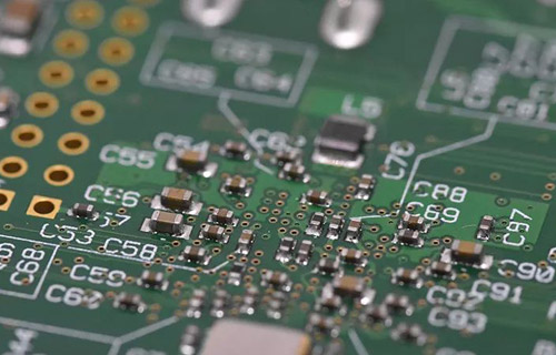
The screen printing layer of PCB board is a text layer. Its function is to facilitate the installation and maintenance of the circuit, and print the required logo patterns and text codes on the upper and lower surfaces of the PCB board, such as component labels and nominal values, component shapes and manufacturer identification, production date, etc.
1. Place
Generally speaking, the screen of resistor, capacitor, tube and other components should not be placed in four directions, which will lead to tiredness when looking at the screen during commissioning, maintenance and welding (the board should rotate in several directions). Therefore, it is recommended to place them in two directions, as shown in the figure below. In this way, it is very important to view the screen.

2. The via shall not be punched on the screen as much as possible.
3. The silkscreen shall not be pressed on the high-speed signal line (such as clock line).
This recommendation applies to high-speed signal lines at the top or bottom, as these signal lines can be considered as microstrip lines. The speed (phase speed) of the signal running on the microstrip line is related to the medium. If the silk screen is pressed on the line, the medium will become uneven, leading to the change of phase velocity, which finally shows that the impedance is discontinuous, affecting the signal quality. Of course, the signal line of the inner layer will not have this problem.
4. The reading direction of silkscreen should be consistent with the use direction.
The reading direction of screen printing is consistent with the use direction of the chip, mainly in the welding process to reduce the probability of reverse welding. Others, such as electrolytic capacitors, do not follow this recommendation because you can specify positive and negative polarity.
5. The pin number shall be clearly marked on the silkscreen.
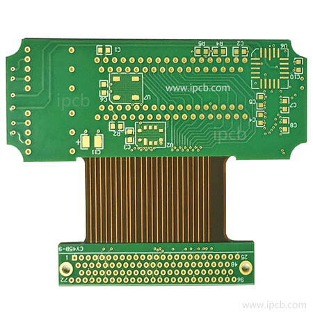
There are 4 pin numbers on the P3 connector, which is convenient for debugging and installation. In addition, it is better to mark the places with dense pins, such as chips, FPC sockets, etc. At the same time, the reading direction of P3 is consistent with the use direction of the connector.
6. Specially packaged silk screen.
For special packages such as BGA and QFN, the size of the silkscreen should be exactly the same as that of the chip (as shown in the figure below), otherwise, it will be difficult to align, which will affect the welding.
7. Screen printing of mounting holes.
Here, the silkscreen of screws is added near the mounting hole, and the length and total number of screws are also marked for easy installation.
8. The ambiguity of silk screen.
The most commonly used is RS232. Many people will mark RX and TX, but there are also RX and TX on the PC side. When to use crossover lines and when not? This leads to the fuzziness of screen printing, making people silly to distinguish. Here, two arrows are added to indicate the direction of the signal (as shown in the figure below), so that you can see at a glance how to connect the wires. Not only RS232 can do this, but others, such as SPI, with transceiver signal line, can do this.
The screen printing layer is a text layer, which belongs to the top layer of PCB board and is generally used for marking. The correct character layout principle of screen printing layer is: "no ambiguity, no stitch, beautiful and generous". This is to facilitate the installation and maintenance of the circuit, and to print the required marks and special layers of character coding on the upper and lower surfaces of the printing plate.
1) All components, mounting holes and positioning holes are provided with corresponding silk screen labels. To facilitate the installation of boards, all components, mounting holes and positioning holes are provided with corresponding silk screen labels. The mounting holes on the PCB are screen printed H1 and Hn. Next identification.
2) Silkscreen is displayed from left to right and from bottom to top. For polar devices, such as electrolytic capacitors and diodes, please ensure that the direction of each functional unit is consistent.
3) There is no silkscreen on the solder pad or tin bath to be lined with tin, and the equipment position number should not be blocked by the equipment after installation. (High density, except PCB without screen printing)
4) In order to ensure the welding reliability of the equipment, it is required that there is no screen printing on the bonding pad of the equipment. In order to ensure the continuity of tin lining, it is required that there is no silkscreen on the tin lining; To facilitate the installation and maintenance of the equipment, the position number of the equipment after installation shall not be blocked by the equipment. The silkscreen shall not be pressed on the through hole or bonding pad to avoid partial silk screen loss caused by opening and blocking the welding window, which will affect the training. The screen spacing is greater than 5mil.
5) The polarity of polar components is clearly shown on the silkscreen diagram, and the polarity direction marks are easy to identify.
6) The number of photo files of PCB board is correct, each layer should have correct output, and there should be complete layer output.
7) The identifier of components on PCB must be consistent with that in BOM list.
8) The direction of the directional connector is clearly indicated on the silkscreen.
9) The PCB board shall be provided with barcode position identification. If the space on the PCB board allows, the PCB board shall be provided with 42 * 6 barcode silk screen frame. The position of the barcode shall be convenient for scanning.
10) The silkscreen position of PCB name, date, version number and other information of the finished board shall be clear. PCB board documents shall be printed with board name, date, version number and other board information, with clear and eye-catching location.