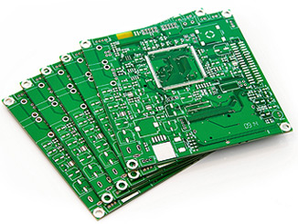
The so-called lead-free soldering iron welding means that the solder used for welding fr4 pcb is not allowed to contain Pb, while the content of Pb in the current commonly used solder is up to 40%. The key to realize lead-free soldering is to find a lead-free lead-free soldering tin that can replace the current lead-free soldering tin. Lead solder has been used for hundreds of years because it has a series of excellent properties, low price and sufficient reserves.
In the past 20 years, the electronic industry and related scientific and technological circles all over the world have invested a lot of manpower and material resources to research and develop lead-free solder. However, due to the stringent requirements of this new electronic material, the progress is not ideal. At present, only Sn-Ag-Cu alloy with relatively good properties can be used as a temporary substitute for Sn-Pb alloy.

Sn-Ag-Cu solder is the main type of lead-free soldering iron currently used. Sn-Ag-Cu alloys are usually SAC305-Sn-3.OAg-0.5Cu and SAC405-Sn-4.OAg-0.5Cu. Compared with 63/37Sn-Pb solder, SAC305 and SAC405 have the following fatal defects:
1) High melting point (SAC is about 220 ℃, Sn-Pb is about 183 ℃);
2) Poor wettability (the wettability of SAC is equivalent to about 70% of Sn-Pb).
The main problem brought about by the improvement of the melting point of lead-free solder is to reduce the process window, that is, from 57~67 ℃ (A) for Sn-Pb solder to 23~33 ℃ (B), thus significantly reducing the variable range of the soldering operation temperature. This not only brings difficulties to the process, but also easily endangers the performance of the substrate and components due to over-temperature. In addition, the hole wettability of error-free solder is poor, which increases the difficulty of lead-free soldering iron welding. In order to meet the needs of lead-free soldering iron welding, the current main countermeasures are as follows:
1) Conduct technical training for operators, first understand the characteristics of lead-free soldering iron in theory, and make full preparation in consciousness.
2) The electric soldering iron with PID temperature control ensures the stability and correctness of the temperature of the electric soldering iron.
3) Select the solder wire. Sn-Ag-Cu solder wire is preferred, in which the content of Ag can be 1%, not necessarily 3%~4%. The diameter of solder wire can be thick or thick, and Sn-Ag-Cu-In-X solder wire can be selected if necessary.
4) Practice operation skills. During welding, add solder to the base metal for a certain preheating time (generally no more than 3s), and be attentive and cautious during operation.
Workflow of reflow soldering:
Stage 1: The temperature must rise at a rate of about 3 ℃ per second to limit the boiling and drop of solvent in the tin sound. If the temperature rises too fast, the solvent will boil, which will cause the metal powder in the tin blue to splash everywhere, making it form small tin beads after cooling and curing, affecting the electrical performance of the product. In addition, some electronic components are sensitive to temperature. If the external temperature of the components rises too fast, the components will burst.
Stage 2: The flux is active, and the chemical cleaning action begins. The same cleaning action will occur for water-soluble flux and wash-free flux, but the temperature is slightly different. At this time, the flux in the solder paste will quickly destroy the oxide on the surface of the welding material and the anti-welding surface of the fr4 pcb pad, making the welding end of the component fully contact with the fr4 pcb pad.
Stage 3: The temperature continues to rise, and the solder particles first melt separately, and begin the "rush" process of liquefaction and surface tin absorption. In this way, cover all possible surfaces upward and start to form solder joints.
Stage 4: This stage is the most important. When all the individual solder particles are melted and combined to form liquid tin, the surface tension begins to form the surface direction of the solder leg. If the gap between the component pin and the fr4 pcb pad exceeds 4mil, it is very likely that the pin and pad will be separated due to the surface tension, which will cause the field open circuit.