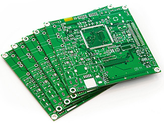
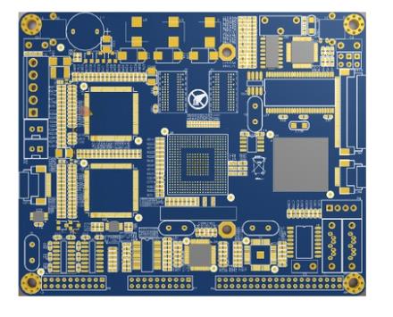
In order to ensure the quality and reduce the cost in the mass production of SMT, online testing is indispensable. In order to ensure the smooth progress of the test work, the design of test points and test holes (electrical connection holes for the electrical performance test of fr4 pcb and fr4 pcb components) should be considered in the design of fr4 pcb.
1) Contact reliability test design. In principle, the test points should be set on the same side and should be evenly distributed. The pad diameter of the test point is 09mm~1.0mm, and it is matched with the relevant test needle. The center of the test points should fall on the grid, and it should not be designed within 5mm of the edge of the board, and the center distance between adjacent test points should not be less than 1.46mm. No other elements shall be designed between the test points, and the distance between the test points and the element pad shall not be less than 1mm to prevent short circuit between the elements or test points, and the test points shall not be coated with any insulating layer. In principle, the test hole can be replaced by the process hole, but the test hole should still be designed on the sub-board when testing the single PCB boardof the panel.

2) For electrical reliability test design, all electrical nodes should be provided with test points, that is, the test points should cover all I/O, power supply ground and return signals. Each IC should have test points for power supply and ground. If there is more than one power supply and ground of the device, test points should be added separately. The power supply and ground of an integrated block should be placed within 2.54mm. The IC control line cannot be directly connected to the power supply, ground or common resistance, For VLSI and ASIC devices with boundary scan devices, auxiliary test points to realize boundary scan function shall be added, such as clock, mode, data serial input/output terminal, reset terminal, to meet the requirements of testing the internal functional logic of the device itself.
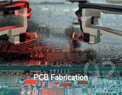
With the wide application of 0201 chip components and 0.3 Pinch integrated circuits, enterprises have higher and higher requirements for product quality. Visual inspection alone cannot ensure product quality. At this time, AOI technology came into being. As a newcomer in the SMT family, AOI effectively solved the difficult problem of surface mount quality detection. AOI has many similarities with the printing press and mounting machine mentioned before, but it is not a production equipment like printing press and mounting machine. Although it is not a production equipment, it has an inseparable relationship with production. This task enables students to master the working principle of AOI through a comprehensive introduction to it.
1. Classification of AOI
The full name of AOI is Automatic Optical Inspection (AOI), which is based on the optical principle to detect the common defects encountered in welding production. AOI is a new testing technology that has only been used in recent years, but has developed rapidly. At present, many factories have launched AOI testing equipment. AOI refers to the position in the reproduction line, which can be divided into online and offline AOI. Although there is division of labor, their working principles are the same.
1) Online: optical detector that can be put on the assembly line and used at the same time with other equipment on the SMT assembly line. The rhythm is the same as the production rhythm of other equipment on the production line. It can be placed at different positions on the production line according to the different purposes of testing. Online AOI adopts 100% full inspection detection method, with high degree of automation, and automatically completes all detection along with the pipeline. The level of concern about ESD is low, because it is an automatic operation, and this problem is basically not considered in the detection process. The manual labor intensity of online AOI is also very low, and no manual assistance is required except for equipment programming. And there is no pollution.
2) Offline AOI: It is an optical detector that can not be placed on the assembly line and used with the SMT assembly line, but can be placed in other positions to detect the fr4 pcb on the SMT assembly line. The offline inspection method is spot check or batch spot check. It has a moderate degree of automation and requires manual assistance to complete the inspection. ESD concerns are high because workers are required to assist in the inspection process and sensitive components need to be handled with extra care. During the use of offline AOI, each board needs to be manually put in and taken out after inspection. Compared with online AOI, offline AOI will cause light pollution, and the inspector will be stimulated by high-brightness light source for a long time in close contact.
2. Structure of AOI
Both online AOI and offline AOI have the same structure and principle. They are usually composed of image acquisition, motion control system, image processing system and data processing system. Compared with other SMT devices, AOI structure is relatively simple.