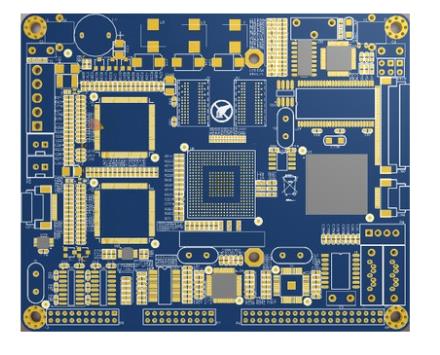
1、fr4 pcb quality inspection
1) X-ray inspection
After assembly, X-ray can be used to see the bridging, open circuit, insufficient solder, excessive solder, ball drop, loss of huai, popcorn, and the most common holes and other defects of the hidden solder joints at the bottom of BGA.
2) Scanning ultrasonic microscopy
The completed assembly board can use SAM scanning to check all kinds of hidden situations, and the packaging industry can detect all kinds of hidden holes and layers. This SAM method can be divided into three scanning and imaging methods: A (point), B (line) and C (plane), of which C-SAM plane scanning is the most commonly used.

3) Side view method
The side visual inspection of optical amplification can be carried out for small things in the restricted dead angle area. BGA's ball foot welding can be used to check the outer ring. In this method, the prism is rotated 90° to focus the lens, and the CCD with high resolution is used to transmit the picture. The magnification is between 50X and 200X, and positive light and backlight observation can also be carried out. It can be seen that the solder joint conditions include: overall appearance, tin eating, solder joint shape, solder joint surface pattern, flux residue and other defects. However, the inner sphere of BGA can not be seen by this method. It needs to be directly observed by using a very thin fiber tube endoscope. However, although the idea is good, it is not practical. It is not only expensive but also easy to break.
4) Screwdriver strength measurement
Use the torsion moment generated by the rotation of the special screwdriver to jack up and tear the solder joint to observe its strength. Although this method can find defects such as floating of solder joint, interface splitting, or weld body cracking, it is not effective for thin plate.
5) Microsection method
This method requires not only various facilities for sample cutting and preparation, but also sophisticated skills and rich interpretation knowledge to find out the real problem in a destructive way.
6) Infiltration dyeing method (commonly known as red ink method)
Immerse the sample in the diluted special red dye solution, so that the cracks and small holes of various solder joints are capillary infiltrated, and then dried. When each test ball foot is pulled or pried off by force, it is possible to check whether there are red spots on the section and see how complete the solder joint is? This method is also called Dye and Pry. Its dye solution can also be prepared separately with fluorescent dyes, which will make it easier to see the truth in the ultraviolet environment.
2、Hollow ball foot and other defects
2.1 Causes of solder joint voids
The solder joints formed by various SMT solder pastes will inevitably have holes of different sizes, especially the BGA/CSP ball pin solder joints. After entering the high-heat lead-free soldering, the tendency of the holes is even worse. The causes can be classified into several categories:
2.1.1 Organic materials: the solder paste contains about 10-12% by wt. Among them, more fluxes have the greatest impact. The degree of cracking and gas generation of various fluxes is different, so the one with less gas generation rate should be selected as the best strategy. Secondly, the flux in high heat will adhere to the oxide on the solder surface, so the formation of voids can be reduced if the oxide can be removed quickly. Because lead-free soldering is not good, it will also make the cavity worse.
2.1.2 Solder: When the molten solder contacts with the clean surface to be welded, it will immediately generate IMC and weld firmly. However, this reaction will be affected by the size of the surface tension of the solder. The larger the surface tension, the greater the cohesion, so the adhesion or fluidity required for outward expansion will become worse. Therefore, the organic matter or bubbles in the solder paste solder joint of SAC305 with large surface tension cannot escape from the solder body, but can only be detained in the body and become a cavity. Once the melting point of the solder ball is lower than the solder paste, the holes will float into the ball and gather more.
2.1.3 Surface treatment: if the surface treatment film is easy to be stained with tin, the hole will be reduced, otherwise the tin shrinkage or solder rejection will cause bubbles to gather and form a large hole. As for the interface micro-holes that are easy to cause solder joint cracking, silver immersion is more common. There is a transparent organic film on the surface of silver immersion to prevent silver discoloration; Because the silver layer will rapidly dissolve in liquid tin during welding to form IMC of Ag3Sn5. The remaining organic film will inevitably crack and become tiny holes in strong heat, which is specially called "champagne bubble", so we know that the silver layer should not be too thick and 0.2 μm is better. When the OSP is too thick, the interface micro-holes will also be generated, and the skin film shall not exceed 0.4 μm。
2.1.4 Sometimes the welding pad with large area is also prone to cavities or microholes. At this time, the split method can be used to add several outgoing ditches, or the green paint cross line can be printed to facilitate the escape of gas and avoid cavities. As for the holes caused by micro-blind holes, of course, the best choice is to fill the holes with electroplated copper. Other effective ways to reduce cavities are to avoid water absorption of solder paste, prevent excessive roughness of copper surface or organic residual film.
2.2 Hole acceptance specification
Too many holes in the ball foot will affect its conductivity and heat transfer, and the reliability of the solder joint is also poor. The upper limit of the allowable acceptance of the hole diameter in the top section is 25%, and the diameter of this 25% is about 6% of the total contact area, and the size of the hole must be calculated together. The voids in the interface between the ball foot and the carrier plate or the upper and lower welding pads of the fr4 pcb are actually the main cause of cracking.
2.3 Cavity classification
BGA holes can be divided into five categories according to their location and source. In terms of conscience, the classification of holes in the list chart is very rough, and will be revised in the future.
2.4 Bridging
The reasons for bridging and short circuit between ball pins may be: poor solder paste printing, incorrect placement of components, manual adjustment after placement, or tin splashing during fusion welding. The reasons for open include poor printing of solder paste, adjustment after placement, poor coplanarity, or poor soldering of solder pad on the board.
2.5 Cold elasticity
The main reason for Cold Solder is that due to insufficient heat, there is no IMC formed between the solder and the surface to be welded, or the number and thickness of IMC are insufficient, so that it can not show strong strength. This defect can only be examined carefully fr4 pcb by optical microscope and microsection.