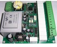
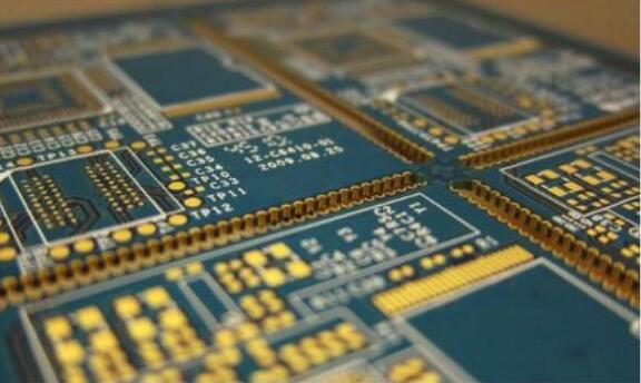
With the continuous improvement and perfection of technology in China’s increasingly developing economic environment, SMD processing may not be very familiar to everyone. In fact, it is a sensitive component and the process is more complicated. Then everyone knows SMD Are there any standard requirements for processing? What are the reasons for the appearance of tin beads?
PCBA passes through SMT on the empty PCB board, and then goes through the production process of DIP plug-in. It will involve a lot of fine and complicated process and some sensitive components. If the operation is not standardized, it will cause process defects or components. Damage, affecting product quality and increasing processing costs. Therefore, in the PCBA patch processing, it is necessary to comply with the relevant operating rules and operate in strict accordance with the requirements.
1. There should not be any food or drink in the PCBA work area, smoking is prohibited, no sundries that are not related to work should be placed, and the workbench should be kept clean and tidy.

2. During PCBA patch processing, the surface to be soldered cannot be taken with bare hands or fingers, because the grease secreted by human hands will reduce solderability and easily lead to soldering defects.
3. The operation steps of PCBA and components are reduced to the limit to prevent danger. In assembly areas where gloves must be used, soiled gloves will cause contamination, so gloves must be replaced frequently when necessary.
4. Do not use skin-protecting oils to coat hands or various silicone-containing detergents, as they can cause problems in solderability and adhesion of conformal coatings. A specially formulated detergent for PCBA soldering surface is available.
5. Components and PCBA that are sensitive to EOS/ESD must be marked with appropriate EOS/ESD marks to avoid confusion with other components. In addition, in order to prevent ESD and EOS from endangering sensitive components, all operations, assembly and testing must be completed on a workbench that can control static electricity.
6. Regularly check EOS/ESD workbenches to confirm that they can work normally (anti-static). The various dangers of EOS/ESD components can be caused by incorrect grounding methods or oxides in the ground connection parts. Therefore, special protection should be given to the "third line" grounding terminal joints.
7. It is forbidden to stack PCBA, otherwise physical damage will occur. There should be dedicated various brackets on the assembly work surface, and they should be placed according to the type.
In PCBA patch processing, these operating rules should be strictly followed, and correct operation can ensure the final use quality of the product, and reduce the damage of components and reduce the cost.
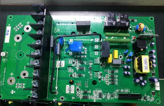
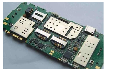
The tin bead phenomenon during PCBA processing is one of the main defects in production. Because of its many causes and difficult to control, it often troubles PCBA processing patch engineers and technicians.
1. The tin beads mainly appear on one side of the chip resistance-capacitance component, and sometimes also appear near the pins of the chip IC. Tin beads not only affect the appearance of board-level products, but more importantly, due to the dense components on the printed board, there is a risk of short circuits during use, which affects the quality of electronic products. There are many reasons for the production of tin beads, which are often caused by one or more factors. Therefore, prevention and improvement must be done one by one to better control them.
2. Tin ball refers to some large solder balls before the solder paste is soldered. The solder paste may be outside the printed pad due to various reasons such as collapse and squeeze. When soldering, these may exceed the pad. The solder paste fails to fuse with the solder paste on the pad during the soldering process and comes out independently, and is formed in the component body or near the pad.
3. However, most of the solder balls occur on both sides of the chip component. Take the chip component with a square pad design as an example. As shown in the figure above, after the solder paste is printed, if the solder paste exceeds, it is easy to produce solder beads. Melting with the solder paste on the pad part will not form solder beads.
However, when the amount of solder is large, the component placement pressure will squeeze the solder paste under the component body (insulator), and it will be melted during reflow soldering. Due to the surface energy, the melted solder paste gathers into a ball, which tends to raise the component., But this force is extremely small, and it is squeezed to both sides of the component by the gravity of the component, separated from the pad, and formed tin beads when cooled. If the component has high gravity and more solder paste is squeezed out, multiple solder balls may even be formed.
4. According to the reasons for the formation of tin beads, the main factors that affect the production of tin beads in the PCBA processing patch production process are:
⑴The design of stencil opening and land pattern.
⑵Steel mesh cleaning.
⑶Repeat accuracy of PCBA placement machine.
⑷Temperature curve of reflow oven.
⑸ Patch pressure.
⑹The amount of solder paste outside the pad.