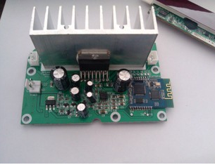
Considerations of PCBA proofing on the size of the pad aperture
When Shenzhen PCB proofing plug-in component pads, the size of the pad should be suitable for PCB proofing. If the pad is too large, the spreading area of the solder is larger, and the solder joint formed is not full, while the surface tension of the copper foil of the smaller pad is too small, and the solder joint formed is a non-wetting solder joint. The matching gap between the aperture and the component line is too large, and it is easy to solder. When the aperture is 0.05~0.2mm wider than the lead and 2~2.5 times the diameter of the pad, it is an ideal condition for welding.
Shenzhen PCB proofing according to the requirements of the pad is to achieve the minimum diameter, which is at least 0.5mm larger than the maximum diameter of the small hole flange of the welding terminal. Test pads must be provided for all nodes in accordance with ANSI/IPC 2221 requirements. A node is an electrical connection point between two or more components. A test pad needs a signal name (node signal name), the x-y coordinate axis related to the reference point of the printed circuit board, and the coordinate position of the test pad (indicating on which side of the printed circuit board the test pad is located).

The aspect ratio of plated through holes has an important influence on the manufacturer's ability to plate through holes effectively, and it is also important to ensure the reliability of the PTH/PTV structure. When the size of the hole is less than 1/4 of the thickness of the basic circuit board, the tolerance should be increased by 0.05mm. When the hole diameter is 0.35mm or less and the aspect ratio is 4:1 or greater, the manufacturer should use appropriate methods to cover or block the plated through holes to prevent solder from entering. Generally speaking, the ratio of the thickness of the printed circuit board to the pitch of the plated through holes should be less than 5:1.
It is necessary to provide information on fixtures for SMT, as well as the temperature-sealing technology of printed circuit board assembly layout, to promote the in-circuit with the help of "circuit test fixtures" or commonly referred to as "nail bed fixtures". Testability. In order to achieve this goal, you need:
1) The diameter of the test pad dedicated for probing should not be less than 0.9mm.
2) The space around the test pad should be greater than 0.6mm and less than 5mm. If the height of the component is greater than 6.7mm, the test pad should be placed 5mm away from the component.
3) Do not place any components or test pads within 3mm from the edge of the printed circuit board.
4) The test pad should be placed in the center of a 2.5mm hole in a grid. If possible, allow the use of standard probes and a more reliable fixture.
5) Do not rely on the edge of the connector pointer for pad testing. The test probe can easily damage the gold-plated pointer.
6) Avoid plated through holes-probing on both sides of the printed circuit board. Put the test tip through the hole on the non-component/soldering surface of the printed circuit board. This approach can allow the use of reliable, less expensive devices. The number of different hole sizes should be kept to a minimum. Our factory is located in China. For decades, Shenzhen has been known as the world's electronics R&D and manufacturing center. Our factory and website are approved by the Chinese government, so you can skip the middlemen and buy products on our website with confidence. Because we are a direct factory, this is the reason why 100% of our old customers continue to purchase oniPCB.