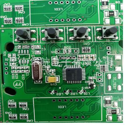
PCB signal line cloth
In the multi-layer printed board wiring, because there are not many wires left in the signal line layer that have not been laid out, adding more layers will cause waste and increase the production workload, and the cost will increase accordingly. To solve this contradiction, you can consider wiring on the electrical (ground) layer. The power layer should be considered first, and the ground layer second. Because it is best to preserve the integrity of the formation.
Treatment of connecting legs in large area conductors
In large-area grounding (electricity), the legs of common components are connected to it. The treatment of the connecting legs needs to be considered comprehensively. In terms of electrical performance, it is better to connect the pads of the component legs to the copper surface. There are some undesirable hidden dangers in the welding and assembly of components, such as: 1. Welding requires high-power heaters. 2. It is easy to cause virtual solder joints. Therefore, both electrical performance and process requirements are made into cross-patterned pads, called heat shields, commonly known as thermal pads (Thermal), so that virtual solder joints may be generated due to excessive cross-section heat during soldering. Sex is greatly reduced. The processing of the power (ground) leg of the multilayer board is the same.
The role of the network system in wiring!

In many CAD systems, wiring is determined by the network system. The grid is too dense and the path has increased, but the step is too small, and the amount of data in the field is too large. This will inevitably have higher requirements for the storage space of the device, and also the computing speed of the computer-based electronic products. Great influence. Some paths are invalid, such as those occupied by the pads of the component legs or by mounting holes and fixed holes. Too sparse grids and too few channels have a great impact on the distribution rate. Therefore, there must be a well-spaced and reasonable grid system to support the wiring.
The distance between the legs of standard components is 0.1 inches (2.54 mm), so the basis of the grid system is generally set to 0.1 inches (2.54 mm) or an integral multiple of less than 0.1 inches, such as: 0.05 inches, 0.025 inches, 0.02 Inches etc.
Design Rule Check (DRC)
After the wiring design is completed, it is necessary to carefully check whether the wiring design meets the rules set by the designer, and at the same time, it is necessary to confirm whether the rules set meet the requirements of the printed board production process. The general inspection has the following aspects:
(1) Whether the distance between line and line, line and component pad, line and through hole, component pad and through hole, through hole and through hole is reasonable, and whether it meets the production requirements.
(2) Is the width of the power line and the ground line appropriate, and is the power supply and the ground line tightly coupled (low wave impedance)? Is there any place in the PCB where the ground wire can be widened?
(3) Whether the best measures have been taken for the key signal lines, such as the shortest length, the protection line is added, and the input line and output line are clearly separated.
(4) Whether there are separate ground wires for the analog circuit and digital circuit part.
(5) Whether the graphics (such as icons and annotations) added to the PCB will cause signal short circuit.
(6) Modify some unsatisfactory linear shapes.
(7) Is there a process line on the PCB? Whether the solder mask meets the requirements of the production process, whether the solder mask size is appropriate, and whether the character logo is pressed on the device pad, so as not to affect the quality of the electrical equipment.
(8) Whether the outer frame edge of the power ground layer in the multilayer board is reduced, such as the copper foil of the power ground layer exposed outside the board, which may cause a short circuit.