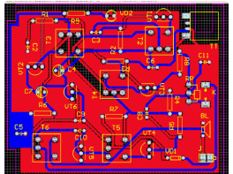
The development and changes of electronic technology will inevitably bring many new problems and new challenges to board-level design. First, due to the increasing physical limits of high-density pins and pin sizes, resulting in low deployment rates; secondly, the timing and signal integrity problems caused by the increase in system clock frequency; thirdly, engineers hope to be able to use the PC platform Use better tools to complete complex and high-performance designs. Therefore, it is not difficult for us to see that PCB board design has the following three trends:
1. The design of high-speed PCB (that is, high clock frequency and fast edge rate) has become the mainstream.
2. Product miniaturization and high performance must face the problem of distribution effect caused by mixed signal design technology (ie digital, analog and RF mixed design) on the same PCB board.
3. The increase in design difficulty has led to the traditional design process and design methods, and the CAD tools on the PC are difficult to meet the current technical challenges. Therefore, the transfer of EDA software tool platform from UNIX to NT platform has become a recognized trend in the industry.
1. High-frequency circuits tend to have high integration and high wiring density. The use of multi-layer boards is not only necessary for wiring, but also an effective means to reduce interference.
2. The less the lead bends between the pins of high-frequency circuit devices, the better. The lead wire of high-frequency circuit wiring is best to adopt a full straight line, which needs to be turned. It can be turned by 45° broken line or arc. This requirement is only used to improve the fixing strength of copper foil in low-frequency circuits, while in high-frequency circuits, this is satisfied. One requirement can reduce the external emission and mutual coupling of high-frequency signals.
3. The shorter the lead of the high-frequency PCB device pin, the better.
4. The fewer lead layers alternate between pins of high-frequency circuit devices, the better. That is, the fewer vias (Via) used in the component connection process, the better. It is measured that one via can bring about 0.5pF distributed capacitance, and reducing the number of vias can significantly increase the speed.
5. For high-frequency PCB wiring, pay attention to the crosstalk introduced by the close parallel routing of the signal lines. If parallel distribution cannot be avoided, a large area can be arranged on the opposite side of the parallel signal lines to greatly reduce interference. Parallel wiring in the same layer is almost unavoidable, but the directions of the wiring in two adjacent layers must be perpendicular to each other.
6. Implement ground wire surround measures for particularly important signal lines or local units.
7. Various signal wires cannot form loops, and ground wires cannot form current loops.
8. At least one high-frequency decoupling capacitor should be installed near each integrated circuit block (IC), and the decoupling capacitor should be as close as possible to the Vcc of the device.
9. When the analog ground wire (AGND), digital ground wire (DGND), etc. are connected to the public ground wire, high-frequency choke should be used. In the actual assembly of the high-frequency choke link, the high-frequency ferrite bead with a wire through the center is often used, which can be used as an inductor in the schematic diagram, and a component package and wiring are defined separately for it in the PCB component library. Move it manually to a suitable position close to the common ground line.

The choice of PCB base material and the setting of the number of PCB layers, the choice of electronic components and the electromagnetic characteristics of electronic components, component layout, and the length and width of the interconnection lines between components, all restrict the electromagnetic compatibility of the PCB. The integrated circuit chip (IC) on the PCB is the main energy source of electromagnetic interference (EMI). Conventional electromagnetic interference (EMI) control technology generally includes: reasonable layout of components, reasonable control of wiring, reasonable configuration of power lines, grounding, filter capacitors, shielding and other measures to suppress electromagnetic interference (EMI) are very effective, Is widely used in engineering practice.
1. The high-frequency digital signal line should be short, generally less than 2inch (5cm), and the shorter the better.
2. The main signal lines are best concentrated in the center of the PCB board.
3. The clock generating circuit should be near the center of the PCB board, and the clock fan-out should be wired in daisy chain or parallel.
4. The power line should be as far away as possible from the high-frequency digital signal line or separated by the ground line. The distribution of the power supply must be low inductance (multi-channel design). The power layer in the multi-layer PCB is adjacent to the ground layer, which is equivalent to a capacitor, which plays a filtering role. The power line and ground line on the same layer should be as close as possible. The copper foil around the power layer should be retracted 20 times the distance between the two plane layers than the ground layer to ensure that the system has better EMC performance. The ground plane should not be divided. If the high-speed signal line is to be divided across the power plane, several low-impedance bridge capacitors should be placed close to the signal line.
5. The wires used for the input and output terminals should try to avoid being adjacent and parallel. It is best to add ground wires between wires to avoid feedback coupling.
6. When the thickness of the copper foil is 50um and the width is 1-1.5mm, the temperature of the wire will be less than 3 degree Celsius through a current of 2A. The wires of the PCB board should be as wide as possible. For integrated circuits, especially the signal wires of digital circuits, usually 4mil-12mil wire width is used, and the wire width of the power line and ground wire is better than 40mil. The minimum spacing of the wires is mainly determined by the insulation resistance and breakdown voltage between the wires in the worst case, usually a wire spacing of more than 4mil is selected. In order to reduce the crosstalk between the wires, the distance between the wires can be increased if necessary, and the ground wire can be inserted as the isolation between the wires.
7. In all layers of the PCB, digital signals can only be routed in the digital part of the circuit board, and analog signals can only be routed in the analog part of the circuit board. The ground of the low-frequency circuit should be grounded in parallel at a single point as much as possible. When the actual wiring is difficult, it can be partially connected in series and then grounded in parallel. To realize the division of analog and digital power supplies, the wiring cannot cross the gap between the divided power supplies. The signal line that must cross the gap between the divided power supplies should be located on the wiring layer close to the large area ground.
8. There are two main electromagnetic compatibility problems caused by the power supply and the ground in the PCB, one is the power noise, and the other is the ground noise. According to the size of the PCB board current, try to enlarge the width of the power line and reduce the loop resistance. At the same time, make the direction of the power line and ground line consistent with the direction of data transmission, which helps to enhance the anti-noise ability. At present, the noise of the power supply and ground plane can only be set to the default value through the measurement of prototype products or the capacity of decoupling capacitor by experienced engineers based on their experience.