Many friends don't know much about PCBA mixing degree and the influence of PCBA mixing degree on SMT chip processing. Next, PCBA chip factory will introduce the influence of PCBA mixing degree on SMT chip processing in detail.
Significance of the concept of PCBA mixing degree
The proposal of the concept of PCBA mixing degree has important guiding significance for the selection of component packaging and the layout of components. The application of this concept, to some extent, can make the packaging process difference on the same assembly surface change. small.
PCBA mixed introduction
The degree of PCBA mixing refers to the degree of difference in the assembly process of various packages on the mounting surface of the PCBA. Specifically, the degree of difference between the process method used and the thickness of the stencil for various package assembly (see Figure 1-7). The greater the degree of difference in assembly process requirements, the greater the degree of mixing, and vice versa; the greater the degree of mixing, the more complicated the process and the higher the cost.

Introduction to the concept of PCBA mixing degree
The degree of PCBA mixing reflects the complexity of the assembly process. The PCBA we usually talk about "good soldering" actually contains two layers. One layer means whether there are components on the PCBA with a narrow process window, such as fine-pitch components; the other layer means the PCBA mounting surface The degree of difference of various packaging assembly processes.
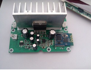
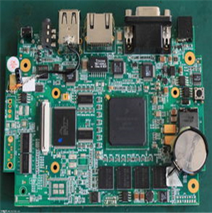
The higher the mixing degree of PCBA, the more difficult it is to optimize the assembly process of each type of package, and the worse the manufacturability. For example, such as mobile phone PCBA (Figure 1-8), although the components used on the mobile phone board are fine pitch or small size components, such as 01005, 0201, 0.4CSP, POP, the assembly of each package is very difficult However, their process requirements are at the same level of complexity, and the degree of mixing of processes is not high. Each package process can be optimized design, and the final assembly yield will be very high; and communication PCBA (such as Figure 1-9), although the size of the components used are relatively large, the degree of mixing of the process is relatively high, and the stepped steel mesh is required for assembly. Due to the limitation of the component layout gap and the difficulty of stencil production, it is difficult to meet the individual needs of each package. Therefore, the final process plan is often a compromise plan that takes care of various packaging process requirements, rather than the most optimized plan. The assembly yield rate will not be very high. This fact also shows that the concept of PCBA mixing degree is extremely important. Packages with similar installation process requirements on the same assembly surface are the basic requirements for package selection. In the hardware design stage, establishing a suitable package is the first step in the design for manufacturability.
Mobile phone PCBA board
PCBA communication board
Measurement and classification of mixing degree
The degree of PCBA mixing is expressed by the maximum difference of the ideal stencil thickness of the components used on the same assembly surface of the PCB (as shown in Figure 1-10). The larger the difference, the greater the degree of mixing and the worse the manufacturability.
PCBA mixing degree measurement
According to the production experience, the mixing degree of PCBA can be divided into four levels, see the table description:
Classification of mixing degree
The greater the difference in thickness of the stencil, the greater the difficulty of process optimization; the greater the difficulty of the process, it does not mean that the production of the stepped stencil is difficult, but the greater the thickness of the stepped stencil, the more difficult it is to guarantee the printing quality of the solder paste; ideally, The step thickness of the step steel mesh should not exceed 0.05mm (2mil).
The relationship between the component pin spacing and the maximum thickness of the steel mesh
The design of the thickness of the steel mesh is mainly considered from two aspects, namely, the component pin spacing and component coplanarity. There is a certain corresponding relationship between the component pin spacing and the area of the steel mesh window, which basically determines the maximum thickness value of the steel mesh that can be used, and the coplanarity of the package determines the minimum thickness value that can be used. Since the thickness of the stencil is not designed based on a single component pin pitch, the degree of mixing cannot be simply determined according to the pitch, but it can be used as a basic reference for component packaging selection. As shown in Figure 1-11, the stencil thickness value corresponding to the pin pitch.
Steel mesh thickness value
The application of the concept of PCBA mixing degree can well solve the selection of component packaging and how to layout the components, and the relationship between mixing degree and process can be used to grasp the difference of assembly process and process cost.
The above is an introduction to the influence of PCBAmixing degree on SMT chip processing