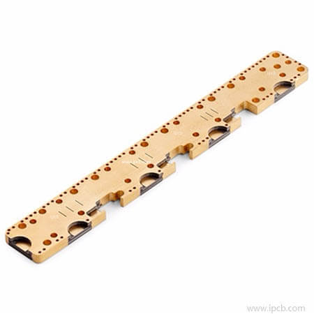
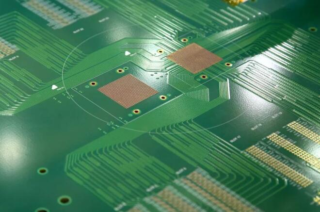
Considerations and defects when PCB soldering BGA
1. a bridge
Fine-pitch BGA components with a pitch of 0.060 inches (1.50 mm) or 0.050 inches (1.0 mm) are not easy to form bridges between adjacent interconnection positions. In addition to the spacing size, there are two other factors that affect the bridge problem.
(1) Excessive amount of solder related to PCB pad size
Due to the mutual affinity of the molten solder between two adjacent locations, when there is too much solder, bridging may occur. The characteristics of each type of BGA are different, depending on the alloy composition used, the melting temperature of the carrier solder ball, the pad design associated with the carrier solder ball, and the weight of the carrier. For example, when other conditions are equal, a high-temperature solder ball carrier (which does not melt during board assembly) is not easy to form a bridge.
(2) Solder paste collapse

When using solder paste as an interconnect material, the collapse of the solder paste during printing and reflow plays an important role in the bridge. The required anti-collapse properties greatly affect the thermal dynamics of the flux/excipient system. Therefore, it is very important to design a flux/excipient system that can provide sufficient surface tension for the solder powder in the chemical system binder that can uniformly wet the surface of the solder powder and provide high adhesion.
2. The PCB solder joints are disconnected or loose
When connecting the BGA to the board, the main factors that affect the disconnection or weakness of the solder joints are as follows: (1) The board is excessively warped
Most PBGA designs must consider partial board warpage from the center to the edge of the component up to 0.005 inches. When the warpage exceeds the required tolerance level, the solder joints may be broken, loose or deformed.
(2) Coplanarity tolerance
The coplanarity required for carrier solder balls is not as critical as fine pitch leads. However, the better coplanarity reduces the disconnection or weakness of the solder joints. The coplanarity is defined as the distance between the highest and lowest solder balls. For PBGA, a coplanarity of 7.8 mils (200μm) is achievable. JEDEC sets the coplanarity standard at 5.9 mils (150μm). It should be pointed out that coplanarity is directly related to the warpage of the board.
(3) Related to wetting
(4) It is related to the clustering of excessively reflowed solder
3. Poor wetting
When soldering the BGA to the motherboard with solder paste, wetting problems may occur between the carrier solder ball and the solder paste or between the solder paste and the pad contact surface. External factors (including BGA manufacturing process, board manufacturing process and subsequent processing, storage and exposure conditions) may cause inappropriate wetting. Wetting problems may also be caused by internal interactions when metal surfaces are in contact, depending on the metal affinity characteristics. The chemical properties and activity of the flux also have a direct effect on wetting.
4. PCB solder clumps
After the PCB board is reflow soldered, if the loose solder mass on the board is not removed, it may cause electrical shorts during work, and it may also make the soldering seam not get enough solder. There are several reasons for the formation of solder bumps:
·For solder powder, substrates or reflow soldering presets are not effectively melted, forming discrete particles that are not agglomerated.
·Before the solder is melted (pre-heating or pre-drying), the solder paste is heated inconsistently, causing the flux activity to degrade. ·The solder paste splashes due to heating too fast, forming discrete solder powder or intruding outside the main soldering area. ·The solder paste is contaminated by moisture or other high "energy" chemicals, which accelerates sputtering.
·During heating, when the solder paste containing ultra-fine solder powder is taken away from the main soldering area by the organic tool, a halo is formed around the pad. · Interaction between solder paste and solder shield.