Circuit board production process: SMT hardware engineers, who want to deal with factories frequently, must fully understand the basic processes and principles of SMT factories.
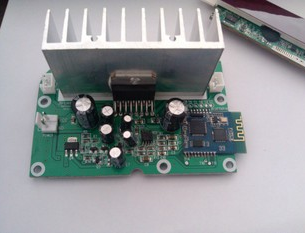
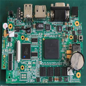
PCBA=PCB Assembled. The assembled PCB. Strictly speaking, PCBA=PCB+components+SMT production+firmware+testing.
With so many components on the circuit board, hand-soldering is definitely not possible, and machines must be used to mount them. No matter whether you have been to the factory or not, you must have seen this picture on TV: a manipulator moved to the circuit board, poke it down several times, and there are components on the circuit board. This is a link in PCB becoming PCBA, SMT.
The machine welding circuit is the same in principle as the manual welding circuit, tinning, placing components, and heating. It's just that the speed of a machine is much higher than that of a human hand, and several components can be placed in one second.
Upper tin:
First, tin the circuit board. As mentioned earlier, there is a paste mask file in the Gerber file, which is used to open the steel mesh. The steel mesh is a thin steel sheet, very flat, with a thickness of about 0.1mm. According to the graphics on the paste mask file, there are corresponding hollow holes. Cover the stencil on the circuit board and align it. At this time, you can see that all the pads that need to be soldered will be exposed. The stencil is the template of the solder paste. Brush a layer of solder paste on the stencil. The solder paste in the holes will be printed on the PCB pads, and there will be no solder where there are no holes. The thickness of the solder paste is the same as the thickness of the steel mesh, which is also as thick as 0.1mm.

The equipment for tinning work is called a "printing machine". Insert the stencil into the machine, and then put the circuit board in. The equipment will automatically hold the circuit board, position it, and hold it tightly under the stencil. There is a brush above the stencil, pushing a lot of solder paste, and going back and forth from the top of the stencil, a layer of solder paste will be piled up at the position of the stencil opening and the groove formed by the circuit board. Take the circuit board off again, and the tin on the circuit board is complete. Next, you need to enter another machine and start placing the components.
Open holes on the stencil, corresponding to the component pads of the circuit board
Print solder paste on the circuit board through the stencil
Patch/SMT
SMT, Surface Mount Technology, surface mount. As the name implies, the components are mounted on the surface of the circuit board. It is called paste because the solder paste has a certain viscosity and can stick to the components even when it is not melted. SMT is also called patch. The meaning of putting the chip on the circuit board.
Because patch is the most important link in the entire PCBA processing process, PCBA processing plants are also called patch plants.
The principle of patching is extremely simple. During manual soldering, the components are clamped and placed on the circuit board with tweezers. The placement machine uses a robot to clamp the components on the circuit board.
However, the actual situation of the patch is very complicated, and the equipment is also very sophisticated. Think about it too, if there is no technical content, why is there always a patch lens on the TV instead of a lens for printing or behind the furnace? We can first look at the following questions:
Where to put the components?
Smaller components, including chips, are stored in tapes. Through the paper or plastic material tape, the components are embedded in the material tape one by one in the same order, and then rolled into a roll. There are many standard-sized holes on the material belt, these holes can be stuck on the gear of the material conveyor, and the gear carries the material forward little by little.
The material conveyor is called Feida. The name is purely transliterated, Feeder. The original intent was a feeder, a breeder. It vividly expresses the function of this thing: feeding materials to the placement machine.
Feida is neatly arranged at both ends of the placement machine. The robot arm of the placement machine is set in accordance with the program to pick up the components from Feida and place them on the circuit board.
For large-size components or bulk materials that are not woven into tapes, they can also be placed on the pallet, and the robot can also pick up materials from the pallet.
How does the manipulator grab such a small component?
In fact, the robotic arm of the placement machine does not rely on fingers to pick up the components, but by vacuum. There are many nozzles on each arm, and each nozzle can suck up one component. If there are more suction nozzles, the robot arm can suck many components in one movement and place it many times, so the production efficiency will be higher.
Components of different sizes have different suction nozzles. It can be seen from high school physics that under the same pressure, the larger the area, the greater the force. Therefore, the suction nozzle for sucking heavier materials such as chips and connectors must be larger., The suction nozzle for the resistance and capacitance should be smaller, and the suction nozzle for 0201 components needs to be smaller.
Heavy objects have greater inertia when moving, so the placement opportunity is divided into several areas. The robot arm in the large component area moves slower, and the small component area moves much faster.
From the principle of picking components in the placement machine, it is not difficult to understand that for pointed components such as pins and thimbles, the materials are shipped with a plastic cover, because they cannot be sucked up without a flat surface. . For components with small openings on the surface such as the USB port, a small piece of high-temperature adhesive tape is attached when leaving the factory. The purpose is to prevent the suction nozzle from leaking.
How does the robot know where to place the components?
In the production materials, there will be a coordinate file indicating the coordinates of each component on the circuit board. Before the on-line placement, the production line engineer will face the production materials and enter the placement information of each component into the operating software of the placement machine. In this way, the placement machine knows which feeder to get how many components and where to place it on the circuit board.
This process is called programming in the factory. The SMT factory has a dedicated program engineer responsible for entering this information. The programming of a circuit board with hundreds of components takes more than half a day.
How to align the circuit board and components?
The circuit board is sent to the placement machine through a conveyor belt. The components are in the material belt, and they are not tightly stuck, and they will shake. The placement machine must be able to determine the precise position of the circuit board and place the components accurately.
The placement machine uses the camera on the robotic arm to identify the circuit board and components. After each component is picked up, it will be photographed. Through the image recognition of this photo, it can be seen whether it is sucked or not. If it is wrong, the system will automatically post it according to the data on the image. The position of the film is compensated to a certain extent, the movement is biased, and the rotation is crooked. Similarly, the circuit board will also be designed with several mark points, a circular pad. The camera can identify the current position of the circuit board according to the position of the pad, and then find the component according to the coordinates of the component relative to the circuit board. Location.
In the process of passing the furnace, the solder paste will melt, and the melted solder paste presents the characteristics of a liquid: it is adsorbed to a place where it can be adsorbed, and tension is generated. It often happens that when the patch is pasted up, it becomes crooked after the oven is over. This is often caused by the different tension between the pads. For example, some PCB pads are large, and some chips have small pads. This need can be solved by controlling the amount of tin and the shape of the tin paste, or adopting the method of dispensing and fixing before the furnace.
There is also a pin-type soldering method, wave soldering, which is still used on old circuit boards and large-size simple circuit boards, specifically for soldering pin circuits. The wave crest of wave soldering means that after the solder is melted, the solder is sprayed out through the nozzle of the equipment, forming a wave shape like a small fountain. Insert the pin of the component into the wave crest, and the solder can be stained and the solder can be absorbed. Solder the pads and pins together.
Now in the field of smart hardware, there are almost no products with full-board plug-in components, most of which are full-board SMT, and occasionally some large-size connectors may require wave soldering.